
Process for producing flexible optical waveguide

a flexible, optical waveguide technology, applied in the direction of optical waveguide light guide, instruments, optics, etc., can solve the problems of distorted cut surface, troublesome light transmission, danger, etc., and achieve enhanced adhesion, easy peeling, and poor adhesion.

Inactive Publication Date: 2006-01-12
NITTO DENKO CORP
View PDF6 Cites 18 Cited by
  • Summary
  • Abstract
  • Description
  • Claims
  • Application Information

AI Technical Summary

Benefits of technology

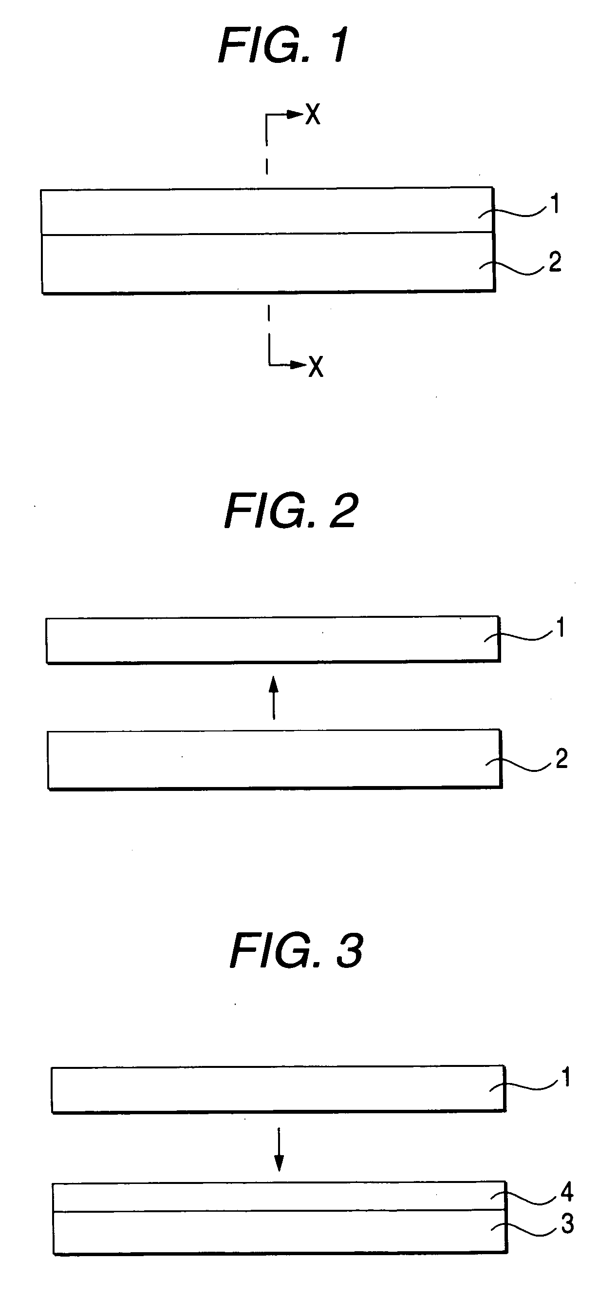
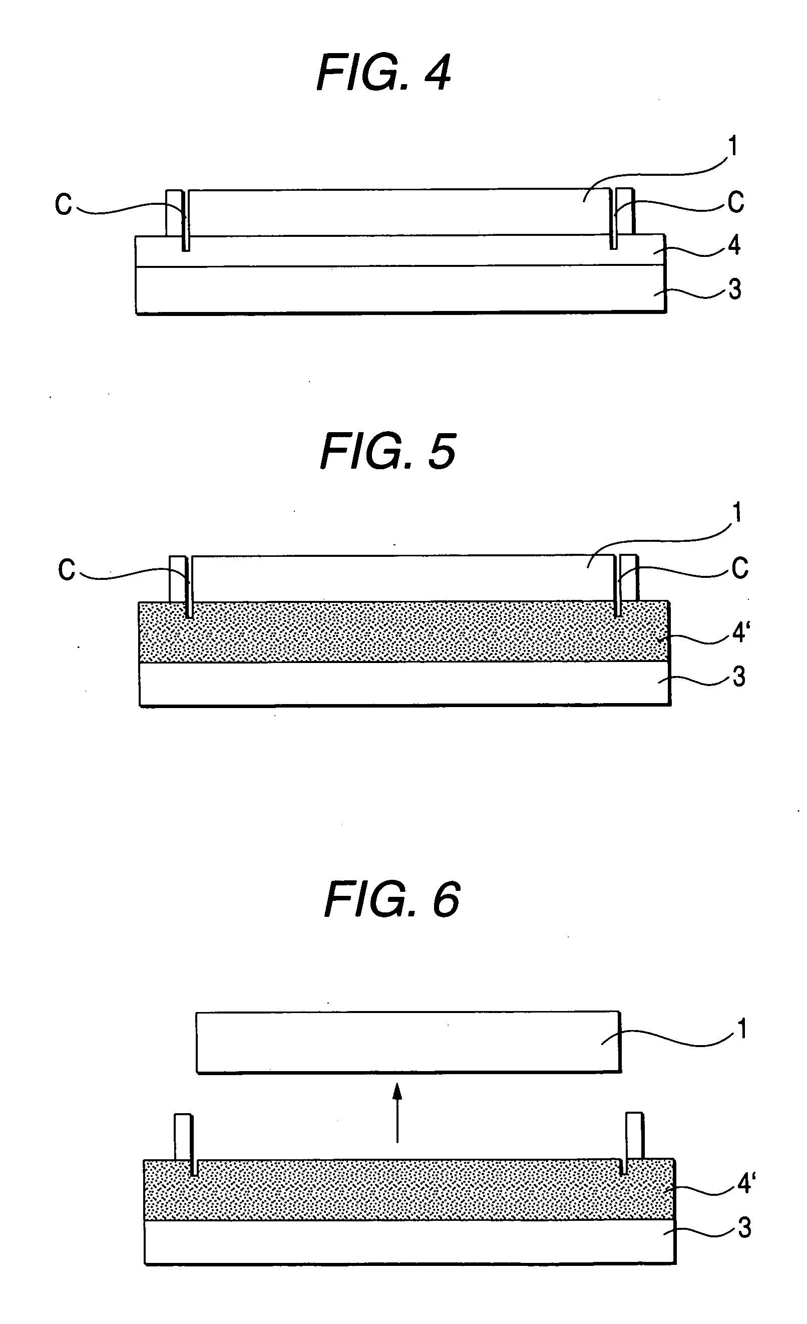
The invention provides a process for safely producing flexible optical waveguides with good light transmission. The process involves peeling off the optical waveguide from the substrate with water, temporarily bonding it to a surface of a pressure-sensitive adhesive layer containing a foaming agent, cutting it into a given length, and then peeling it off the foaming-agent-containing pressure-sensitive adhesive layer after the adhesive layer is allowed to foam by heating. This process ensures that the optical waveguide is securely fixed and can be easily peeled off. The resulting flexible optical waveguide has a smooth finish and good light transmission.

Problems solved by technology

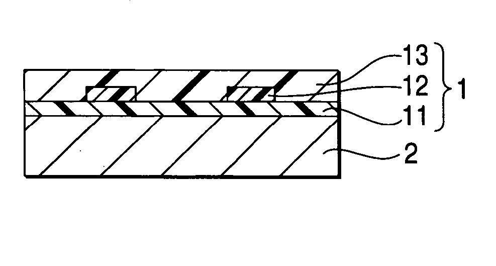
There is hence a problem that separation between the substrate 2 and the undercladding layer 11 occurs during cutting and the optical waveguide 1 moves, resulting in a distorted cut surface.
In case where the optical waveguide 1 has an end surface having a distorted shape, this arouses troubles in light transmission.
However, the technique disclosed in patent document 1 has drawbacks that the peeling operation is accompanied by a danger because hydrochloric acid, which is a strong acid, is used for peeling and that workability is poor.

Method used


Image

  • Process for producing flexible optical waveguide
  • Process for producing flexible optical waveguide
  • Process for producing flexible optical waveguide

Examples


example

Poly(Amic Acid) Solution

[0063] In a 500-mL separable flask equipped with a stirrer, 26.66 g (0.06 mol) of 2,2-bis(3,4 -dicarboxyphenyl)hexafluoropropane dianhydride (6FDA) as an acid dianhydride and 18.54 g (0.058 mol) of 2,2′-bis(trifluoromethyl)benzidine (BTFB) were dissolved in 182.85 g (2.10 mol) of N,N-dimethylacetamide (DMAC) as an organic solvent. Thereafter, the resultant solution was stirred at room temperature (25° C.) for 10 hours to thereby produce a poly(amic acid) solution (polyimide resin precursor solution).

[0064] Subsequently, the poly(amic acid) solution was applied on a 525 μm-thick silicon wafer substrate by spin coating in such an amount as to result in a thickness after heat treatment of 15 μm. The solution applied was dried at 90° C. to thereby form a resin layer comprising a polyimide resin precursor composition. Thereafter, the resin layer was heated at 385° C. under vacuum to thereby complete removal of the solvent remaining in the resin film and imidiza...


PUM


Abstract

The present invention provides a process for producing a flexible optical waveguide which comprises the steps of: immersing a substrate having an optical waveguide formed thereon in water to thereby reduce adhesion between the optical waveguide and the substrate and then peeling the optical waveguide from the substrate; temporarily bonding the peeled optical waveguide to a surface of a pressure-sensitive adhesive layer containing a foaming agent; cutting the temporarily bonded optical waveguide into a given length; allowing the foaming-agent-containing pressure-sensitive adhesive layer after the cutting step to foam by heating, thereby reducing adhesion between the foaming-agent-containing pressure-sensitive adhesive layer and the optical waveguide; and peeling the optical waveguide cut into the given length from the foamed adhesive layer.

Description

FIELD OF THE INVENTION [0001] The present invention relates to a process for producing a flexible optical waveguide which is extensively used in optical communication, optical information processing, and other general optical fields. BACKGROUND OF THE INVENTION [0002] Optical waveguides are incorporated in optical waveguide devices, optical integrated circuits, and optical wiring boards and are in extensive use in optical communication, optical information processing, and other general optical fields. In the case of such an optical waveguide produced on a substrate such as, e.g., silicon or quartz, it is constituted of a core layer which transmits light and one or more cladding layers which have a lower refractive index than the core layer. More specifically, examples thereof include an optical waveguide 1 of a three-layer structure formed on a substrate 2 as shown in FIG. 11. This optical waveguide 1 comprises an undercladding layer 11 formed on the substrate 2, a core layer 12 for...

Claims


Application Information

Patent Timeline
Patent Type & Authority Applications(United States)
IPC IPC(8): G02B6/10
CPCG02B6/12G02B6/25G02B6/1221B05D1/005G02B1/045G02B2006/1215G02B2006/12164G02B2006/12069
Inventor NAITOU, RYUUSUKEMUNE, KAZUNORIMOCHIZUKI, AMANE
Owner NITTO DENKO CORP
Learn More