Magnetoresistive sensor containing self-pinned layer
a self-pinned layer and magnetostriction technology, applied in the field of magnetostriction sensors, can solve the problems of increasing the distance between shielding layers on and under the multilayer film, the gmr effect represented by the resistance change per unit area (ra) cannot be improved, and the structure is unsuitable for recording media having higher linear recording densities, so as to improve the magnetostriction constant, reduce the inversion of the pinned magnetic layer caused, for exampl
- Summary
- Abstract
- Description
- Claims
- Application Information
AI Technical Summary
Benefits of technology
Problems solved by technology
Method used
Image
Examples
first embodiment
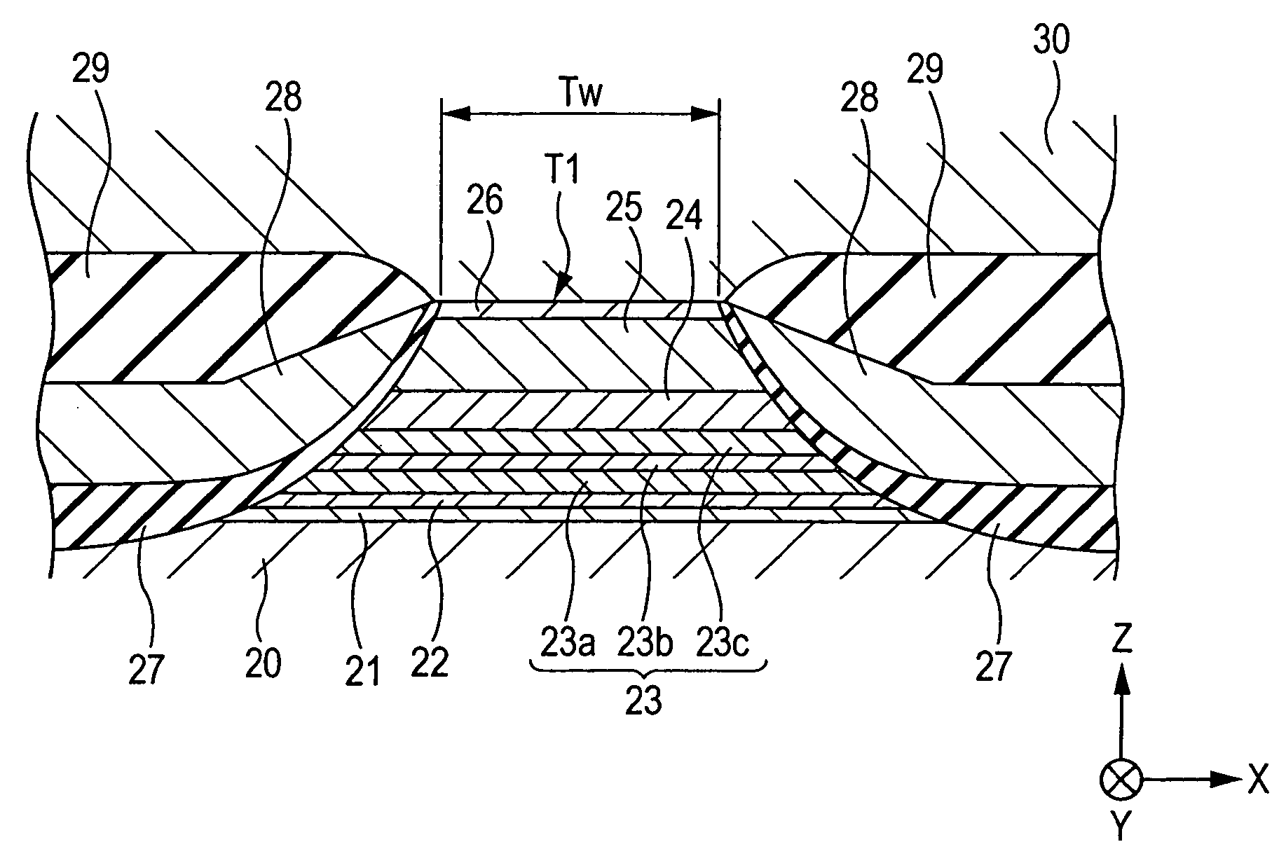
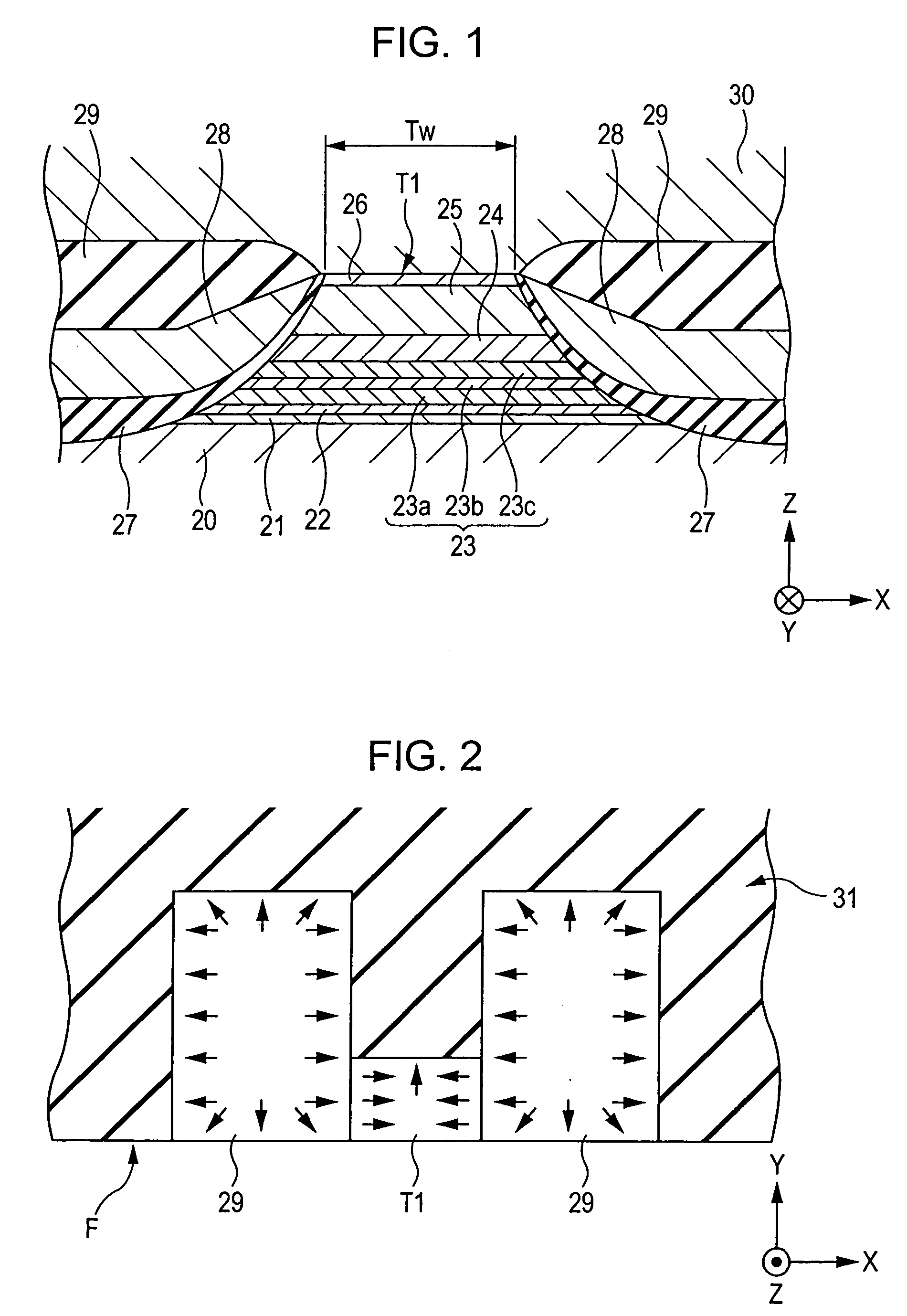
[0063]FIG. 1 is a cross-sectional view of a magnetoresistive sensor according to the present invention, viewed from the side opposite to a recording medium. FIG. 4 is a fragmentary schematic view of the magnetoresistive sensor shown in FIG. 1. In FIG. 4, a first magnetostriction-enhancing layer 22 and a nonmagnetic intermediate sublayer 23b, which are the most characteristic components of the present invention, are indicated by hatched lines.
[0064] In the magnetoresistive sensor shown in FIGS. 1 and 4, a multilayer film T1 is formed on a lower shielding layer 20 made of a magnetic material.
[0065] In the embodiment shown in FIGS. 1 and 4, the multilayer film Ti contains a seed layer 21, the first magnetostriction-enhancing layer 22, a pinned magnetic layer 23, a nonmagnetic material layer 24, a free magnetic layer 25, and a protective layer 26 in this order from the bottom.
[0066] The seed layer 21 is composed of a NiFe alloy, a NiFeCr alloy, Cr, or Ta. For example, the seed layer 2...
fourth embodiment
[0148]FIG. 9 is a schematic view of a multilayer structure T4 (a structure ) different from the multilayer structure T1 in the magnetoresistive sensor of the CPP type shown in FIG. 1.
[0149] Firstly, multilayer structures T5 and T6 shown in FIGS. 10 and 11 will be described. The multilayer structure T5 in FIG. 10 and the multilayer structure T6 in FIG. 11 are comparative examples.
[0150] The multilayer structure T5 shown in FIG. 10 contains a seed layer 21, a first antiferromagnetic layer 50, a first pinned magnetic layer 51, a first nonmagnetic material layer 52, a first free magnetic layer 53, a second nonmagnetic material layer 54 made of Cu, a second pinned magnetic layer 55, a second antiferromagnetic layer 56, a third pinned magnetic layer 57, a third nonmagnetic material layer 58, a second free magnetic layer 59, a third nonmagnetic material layer 60, a fourth pinned magnetic layer 61, a third antiferromagnetic layer 62, and a protective layer 26 in this order from the bottom....
PUM
| Property | Measurement | Unit |
|---|---|---|
| thickness | aaaaa | aaaaa |
| thickness | aaaaa | aaaaa |
| thickness | aaaaa | aaaaa |
Abstract
Description
Claims
Application Information
 - R&D
- Intellectual Property
- Life Sciences
- Materials
- Tech Scout
- Unparalleled Data Quality
- Higher Quality Content
- 60% Fewer Hallucinations
Browse by: Latest US Patents, China's latest patents, Technical Efficacy Thesaurus, Application Domain, Technology Topic, Popular Technical Reports.
© 2025 PatSnap. All rights reserved.Legal|Privacy policy|Modern Slavery Act Transparency Statement|Sitemap|About US| Contact US: help@patsnap.com


