
Multilayer capacitor

a multi-layer capacitor and capacitor technology, applied in the field of multi-layer capacitors, can solve the problems of increasing the current fluctuation of the capacitor, so as to reduce the esl effect and enhance the effect of reducing the total inductan

Active Publication Date: 2005-09-22
TDK CORPARATION
View PDF2 Cites 17 Cited by
  • Summary
  • Abstract
  • Description
  • Claims
  • Application Information

AI Technical Summary

Benefits of technology

[0011] In consideration of the above-described circumstances, it is an object of the present invention to provide a multilayer capacitor realizing reduced total inductance with reduced manufacturing cost.

Problems solved by technology

This has caused the occurrence of a higher-speed and larger current fluctuation in a power source for supplying power to the CPU, and it has become very difficult to control voltage fluctuation accompanying this current fluctuation, within an allowable value range of the power source.
However, today's trend toward a still higher operating frequency of the CPU has resulted in higher-speed and larger current fluctuation, and consequently, equivalent series inductance (ESL) that the multilayer capacitor as a smoothing capacitor itself has become relatively large.
However, in a multilayer capacitor in which a plurality of terminal electrodes are disposed on each of four side faces to be connected to the periphery of a CPU as in the patent document 1 described above, ESL cannot be sufficiently reduced, which has posed a limit on reduction in the total inductance.
However, in manufacturing this multilayer capacitor, it has been necessary to produce a large number of slender through-holes inside the multilayer capacitor.
This as a result makes the manufacture of the multilayer capacitor difficult, which has been a cause of increasing manufacturing cost.

Method used


Image

  • Multilayer capacitor
  • Multilayer capacitor
  • Multilayer capacitor

Examples


Embodiment Construction

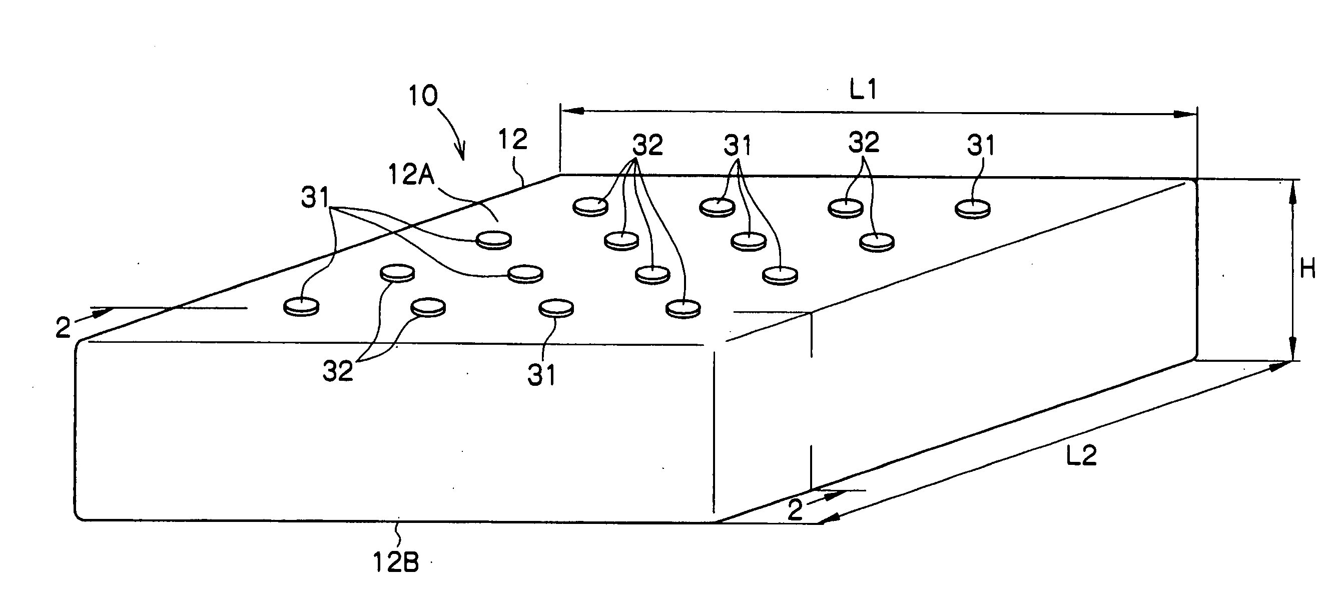
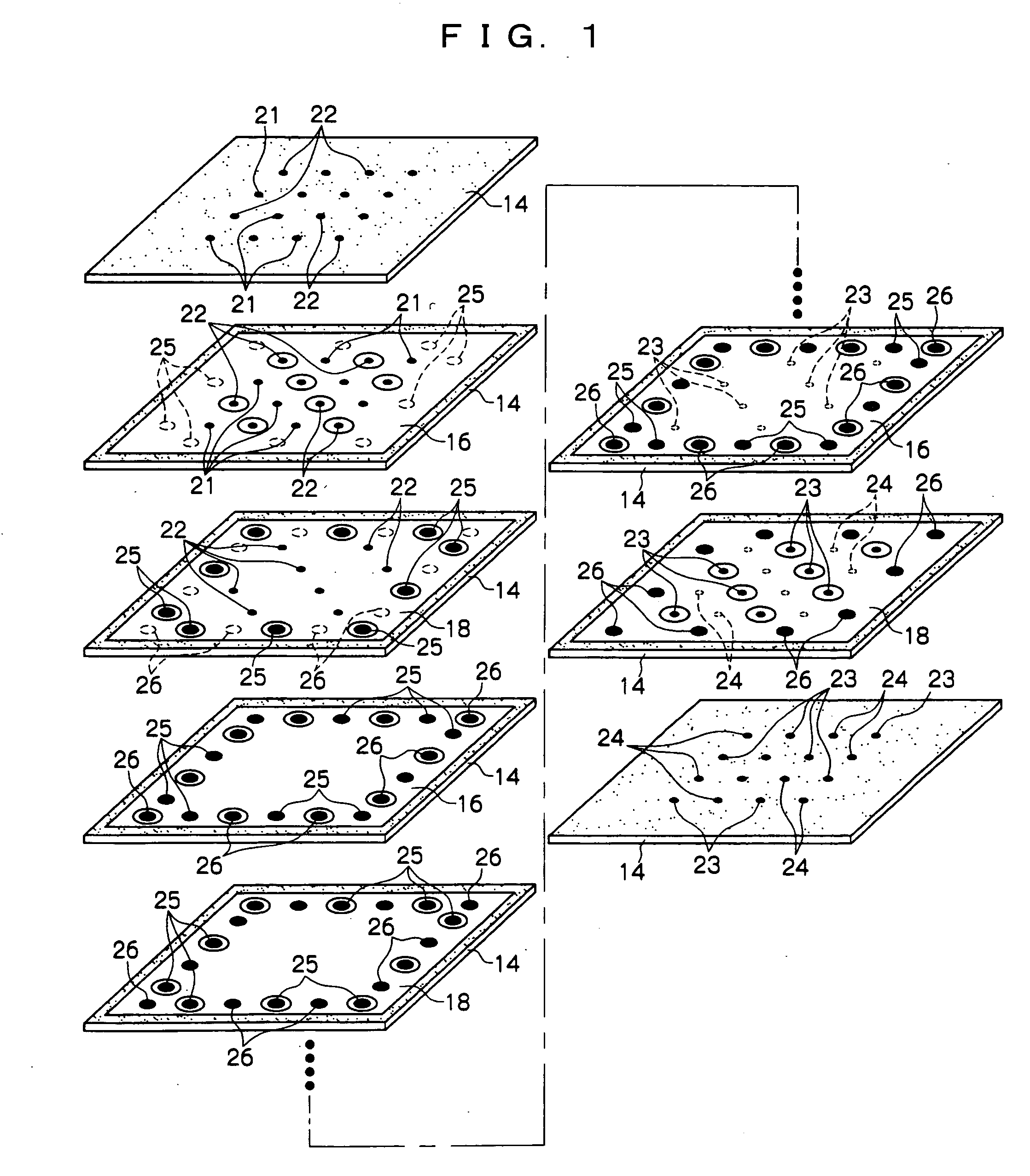
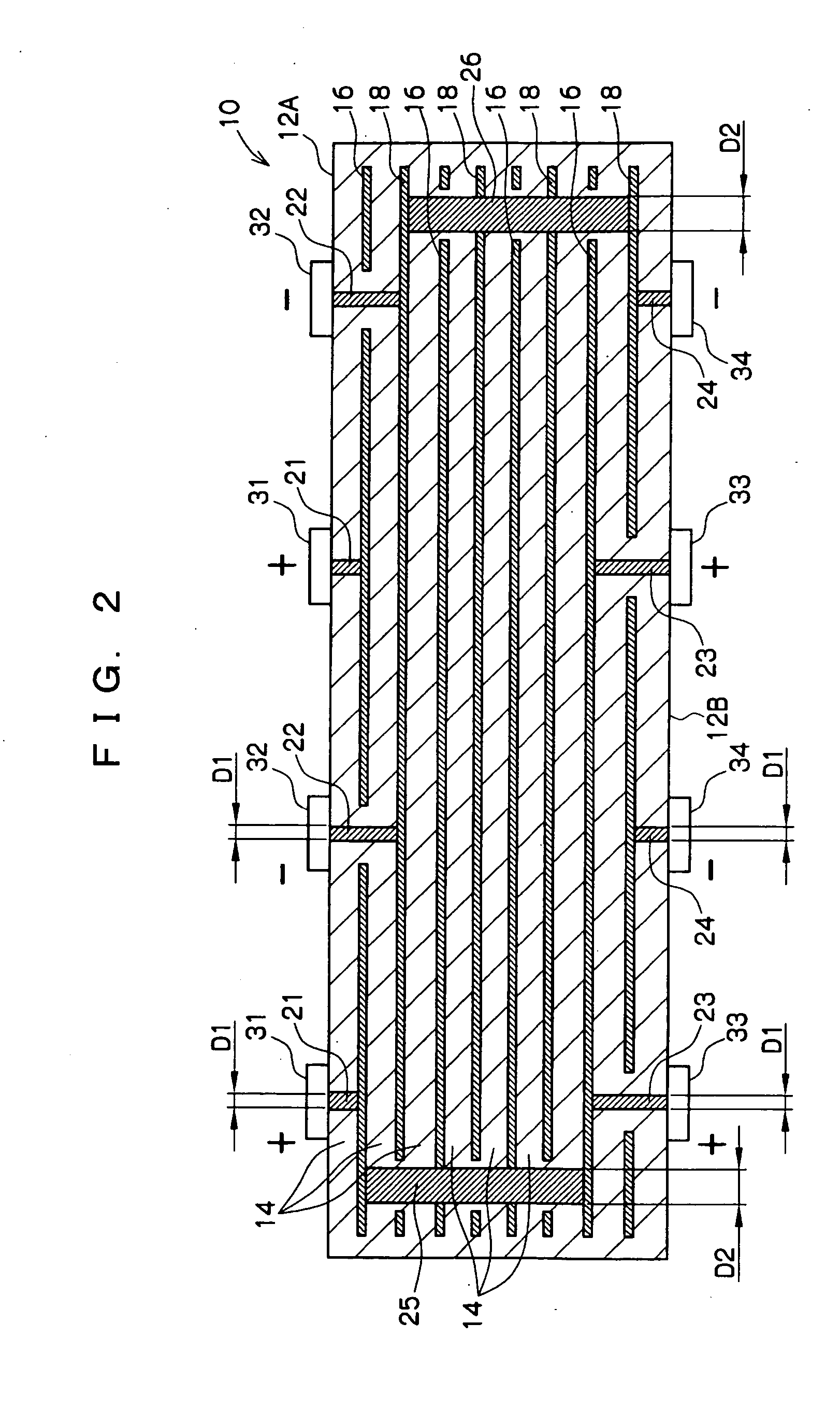
[0036]FIG. 1 to FIG. 3 show a multilayer ceramic chip capacitor 10, which is a first embodiment of a multilayer capacitor according to the present invention, allowing three-dimensional mounting. As shown in these drawings, the multilayer ceramic chip capacitor (hereinafter, abbreviated to a multilayer capacitor) 10 according to this embodiment includes, as a main body portion thereof, a dielectric element 12 being a multilayer body in a rectangular parallelepiped shape that is obtained by sintering a stack of a plurality of ceramic green sheets which are dielectric sheets. Note that longitudinal and lateral dimensions L1, L2 of the dielectric element 12 shown in FIG. 3 are both, for example, 10 mm and a height dimension H is, for example, 0.85 mm.

[0037] As shown in FIG. 1 and FIG. 2, at a predetermined height position in the dielectric element 12, an internal electrode 16 in a planar shape which is a first internal electrode is disposed. In the dielectric element 12, an internal el...


PUM

PropertyMeasurementUnit
diameteraaaaaaaaaa
diameteraaaaaaaaaa
diameter D1aaaaaaaaaa

Abstract

A multilayer capacitor includes: a dielectric element; a plurality of first internal electrodes and a plurality of second internal electrodes alternately arranged in the dielectric element while being separated from each other by dielectric layers; a first outer columnar electrode extending from a surface of the dielectric element to reach the first internal electrode on an outermost layer; a second outer columnar electrode extending from the surface of the dielectric element to reach the second internal electrode on an outermost layer; a first inner columnar electrode connected to all the first internal electrodes and having a cross-sectional area larger than a cross-sectional area of each of the first and second outer columnar electrodes; a second inner columnar electrode connected to all the second internal electrodes and having a cross-sectional area larger than a cross-sectional area of each of the first and second outer columnar electrodes; first external electrodes arranged in an island form on the surface of the dielectric element to be connected to the first outer columnar electrode; and second external electrodes arranged in an island form on the surface of the dielectric element to be connected to the second outer columnar electrode. Therefore, it is possible to obtain a multilayer capacitor that realizes reduced total inductance with reduced manufacturing cost.

Description

BACKGROUND OF THE INVENTION [0001] 1. Field of the Invention [0002] The present invention relates to a multilayer capacitor that realizes reduced total inductance with reduced manufacturing cost, and more particularly, to that suitable for use as a multilayer ceramic chip capacitor capable of reducing voltage fluctuation of a power source of a CPU. [0003] 2. Description of the Related Art [0004] In recent years, due to an improved processing speed and a higher integration degree of a CPU (central processing unit) used for a data processor, its operating frequency is becoming higher and its current consumption is remarkably increasing. In accordance therewith, the operating voltage has been on the decreasing trend due to reduced power consumption. This has caused the occurrence of a higher-speed and larger current fluctuation in a power source for supplying power to the CPU, and it has become very difficult to control voltage fluctuation accompanying this current fluctuation, within ...

Claims


Application Information

Patent Timeline
Patent Type & Authority Applications(United States)
IPC IPC(8): H01G4/12H01G4/06H01G4/232H01G4/252H01G4/30H01G4/38
CPCH01G4/30H01G4/232A45D34/04A45D40/26A45D44/00A45D2034/002A45D2040/0006A45D2200/1009D04H13/00
Inventor TOGASHI, MASAAKIAHIKO, TAISUKE
Owner TDK CORPARATION
Learn More