Component for fabricating an electronic device and method of fabricating an electronic device

a technology of electronic devices and components, applied in the direction of solid-state devices, semiconductor devices, basic electric elements, etc., can solve the problems of limiting product configuration and integrating such electronic devices on the same substrate, and achieve the effects of improving device configuration freedom, efficient reflection of oscillations, and improving the characteristics of film bulk acoustic wave resonators

Inactive Publication Date: 2005-09-01
SNAPTRACK
View PDF3 Cites 8 Cited by
  • Summary
  • Abstract
  • Description
  • Claims
  • Application Information

AI Technical Summary

Benefits of technology

[0014] An acoustic multilayer is preferably provided on the surface of the other substrate. Such provision of the acoustic multilayer improves the characteristics of a film bulk acoustic wave resonator by efficiently reflecting oscillations propagated towards the other substrate.
[0015] Thus, in accordance with this invention, it is possible to form an electronic device on another substrate, that is, a different substrate from the one used for forming the conductive film and the like, thereby greatly increasing the degree of device configuration freedom.

Problems solved by technology

As such, it is often difficult to integrate such an electronic device on the same substrate as other electronic devices, limiting the product configuration.

Method used


Image

  • Component for fabricating an electronic device and method of fabricating an electronic device
  • Component for fabricating an electronic device and method of fabricating an electronic device
  • Component for fabricating an electronic device and method of fabricating an electronic device

Examples


example 1

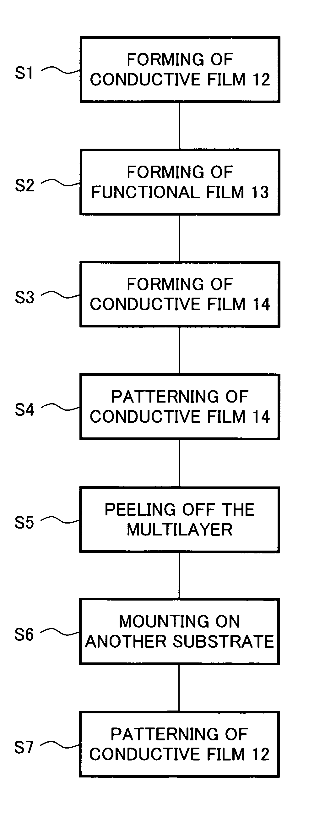
[0070] In Example 1, a plurality of components for fabricating electronic devices having the structure of the component 30 shown in FIG. 3 were fabricated by the following method.

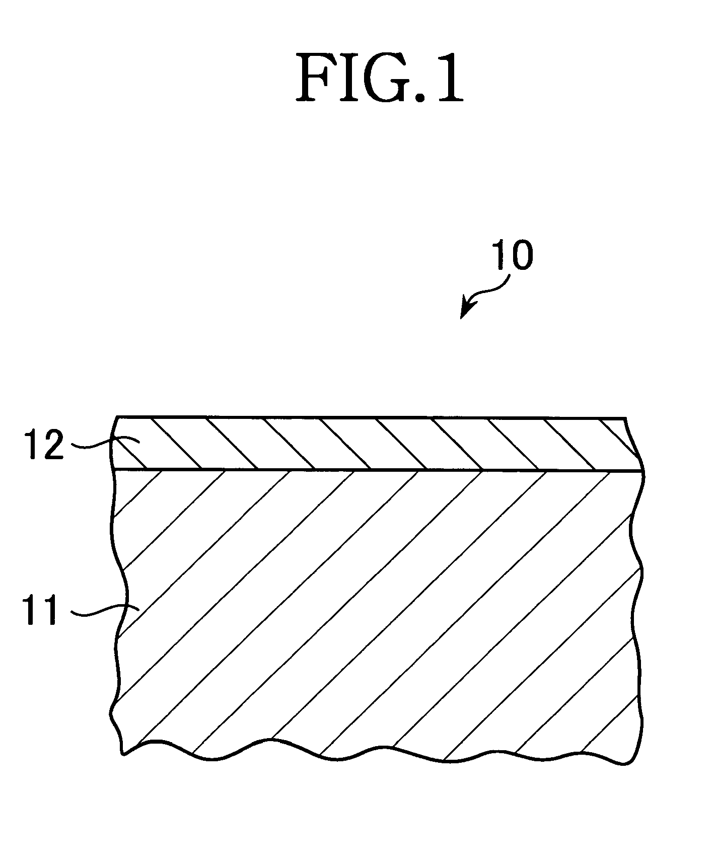
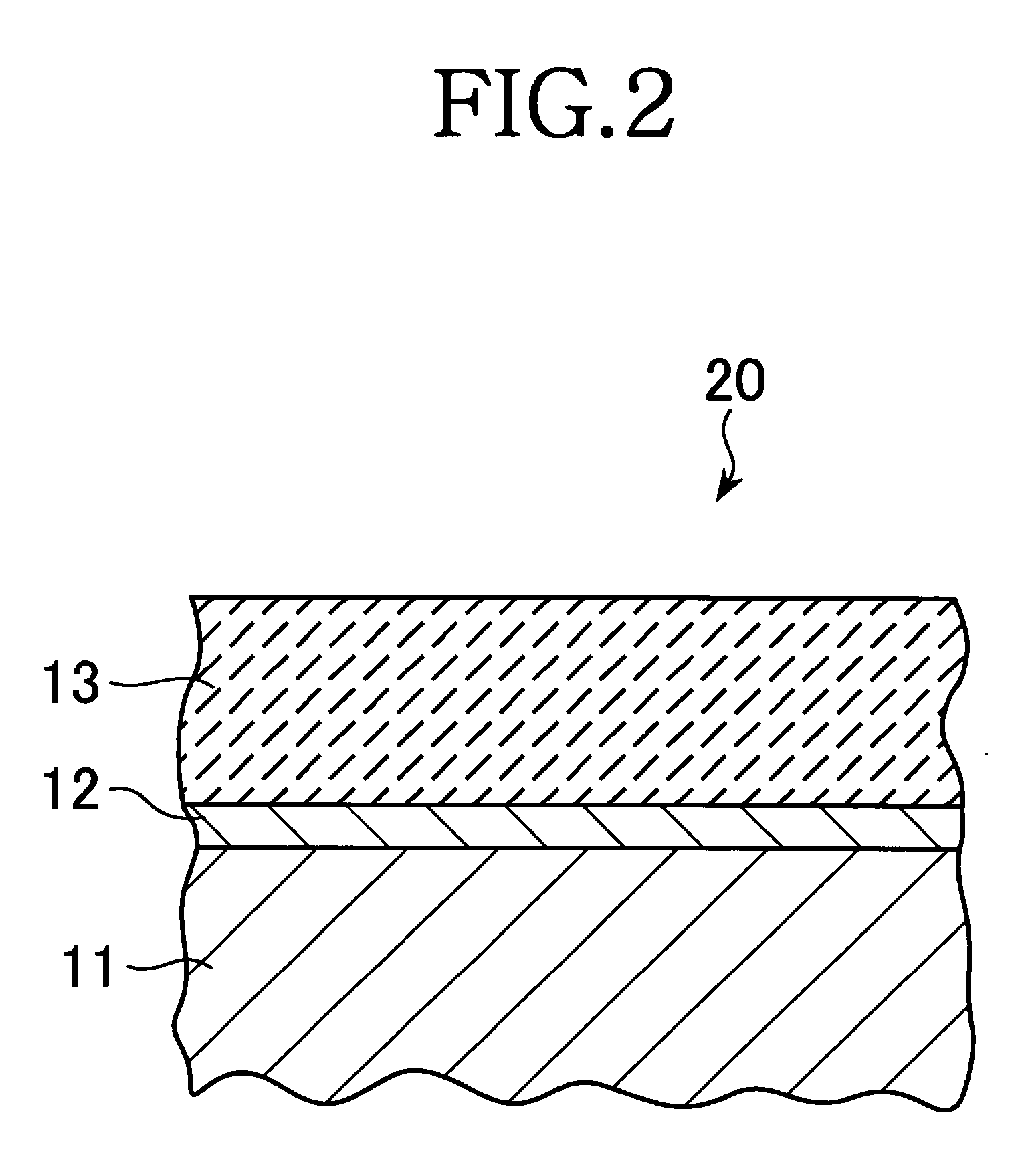
[0071] First, a substrate 11 was prepared from 3-inch-diameter wafer of single crystal silicon with a thermal oxidation film, and a 100 nm thick conductive film 12 of platinum (Pt) was formed on the substrate surface. A substrate temperature of 23° C. was used to form the conductive film 12, using vacuum deposition.

[0072] Next, an 1 μm thick functional film 13 composed of ZnO was formed on the lower conductive film 12 by RF magnetron sputtering.

[0073] Sputtering was then used to form a 300 nm thick conductive film 14 of aluminum (Al) on the functional film 13, thereby completing fabrication of the plurality of components in Example 1.

[0074] The adhesion between the conductive film 12 and the substrate 11 in the components thus fabricated was measured by conducting a peel test, and was found to be 0.005 ...

example 2

[0075] In Example 2, a plurality of components were fabricated in the same manner as in Example 1, except that the substrate temperature during formation of the conductive film 12 was set at 200° C.

[0076] The adhesion between the conductive film 12 and the substrate 11 in the components thus fabricated was measured by conducting a peel test, and found to be 0.025 N / cm. A peel test that was then carried out using ultraviolet curable dicing tape in which the tape together with the multilayer was peeled from the substrate, showed that peeling could be correctly performed with respect to all the components.

example 3

[0077] In Example 3, a plurality of components were fabricated in the same manner as in Example 1, except that the substrate temperature during formation of the conductive film 12 was set at 300° C.

[0078] The adhesion between the conductive film 12 and the substrate 11 in the e components thus fabricated was measured by conducting a peel test, and found to be 0.039 N / cm. A peel test that was then carried out using ultraviolet curable dicing tape in which the tape together with the multilayer was peeled from the substrate, showed that peeling could be correctly performed with respect to all the components.


PUM

PropertyMeasurementUnit
adhesionaaaaaaaaaa
adhesionaaaaaaaaaa
temperatureaaaaaaaaaa

Abstract

A component for fabricating the electronic device comprises a substrate and a conductive film provided on the substrate, in which the adhesion of the conductive film to the substrate is not greater than 0.1 N/cm. The adhesion of the conductive film to the substrate is weak enough to enable the conductive film to be readily peeled from the substrate. This makes it possible to form a component on a substrate other than the substrate used during film formation, thereby greatly increasing the degree of product configuration freedom. If the adhesion of a lower conductive film on the substrate side is made to be not greater than 0.04 N/cm, it becomes very easy to peel the conductive film from the substrate.

Description

TECHNICAL FIELD [0001] The present invention relates to a component for fabricating an electronic device and a method of fabricating the electronic device, and particularly to a component that includes a ferroelectric or piezoelectric functional film and an electrically conductive film provided in the vicinity thereof such as a film capacitors, ferroelectric nonvolatile memories, or film bulk acoustic wave resonators and the like, and to a method of fabricating the electronic device. BACKGROUND OF THE INVENTION [0002] Functional films composed of ferroelectric material or piezoelectric material are used in some electronic devices such as film capacitors, ferroelectric nonvolatile memories, film bulk acoustic wave resonators and the like. A film bulk acoustic wave resonator, for instance, is configured by sandwiching a functional film made of a piezoelectric material between an upper conductive film and a lower conductive film. The film bulk acoustic wave resonator operates as a high...

Claims


Application Information

Patent Timeline
Patent Type & Authority Applications(United States)
IPC IPC(8): H01L21/02H01L21/50H01L41/09H01L23/02H01L41/047H01L41/08H01L41/187H01L41/22H01L41/313H03H3/02H03H9/02H03H9/17
CPCH01L41/047H01L41/316H03H9/175H03H9/02094H03H3/02H10N30/877H10N30/076
Inventor NOGUCHI, TAKAOSAITO, HISATOSHI
Owner SNAPTRACK
Why Eureka
Try Eureka