Semiconductor device and method for fabricating the same

a semiconductor and film technology, applied in the field of semiconductor devices, can solve the problems of deterioration, crack or removal of film, difficult to acquire vivid images with low illumination, light receiving sensitivity, etc., to prevent uneven film thickness of interlayer lenses, prevent cracks or removal, good film thickness uniformity

Inactive Publication Date: 2005-08-18
SHARP KK
View PDF2 Cites 15 Cited by
  • Summary
  • Abstract
  • Description
  • Claims
  • Application Information

AI Technical Summary

Benefits of technology

[0047] Compared to a CVD method, the sputtering method can grow a film at a lower temperature and provides the second transparent film having good film thickness uniformity within the plane of a wafer. Thus, bad influences due to high temperature and film stress on the underlying elements, or unevenness in the film thickness of the interlayer lens can be prevented.
[0048] The second transparent film may be a thin film having a desired refractive index selected from metal compounds and silicon compounds. Alternatively, by sputtering two or more types at the same time, or alternately laminating two ore more types of compound thin films, the refractive index can be varied. For example, a thin film multilayer structure including titanium oxide layers and silicon nitride layers alternately laminated, or a thin film multilayer structure including titanium oxide layers and silicon oxide layers alternately laminated may be used. Such a thin film multilayer structure can relax the film stress and prevent a crack or removal. The thin film multilayer structure also improves the condensing rate compared to the single layer structure by reducing the reflection at the interlayer lens surface. Compared to the CVD method, the sputtering method has a good controllability of the film thickness. Thus, a thin film multilayer structure can be produced with a high controllability.

Problems solved by technology

As the pixel size decreases, the light receiving sensitivity, one of the basic properties of the solid-state image sensing device, deteriorates.
Thus, it is difficult to acquire a picture of a vivid image with a low illuminance.
Therefore, how to improve the light receiving sensitivity per unit pixel is an important challenge to be tackled.
This may cause a crack or removal of the film.
Thus, there is a bad influence on underlying elements due to a high temperature or a film stress, or the film thickness of the inter layer lens becomes uneven.
This causes deterioration of picture quality of the solid-state image sensing device.
If a silicon nitride film is formed with a conventional CVD method, it is extremely difficult to form a transparent film having a refractive index of 2.0 or higher with high uniformity.
This causes the problems that the process steps become complicated and the production cost increases.

Method used


Image

  • Semiconductor device and method for fabricating the same
  • Semiconductor device and method for fabricating the same
  • Semiconductor device and method for fabricating the same

Examples


Embodiment Construction

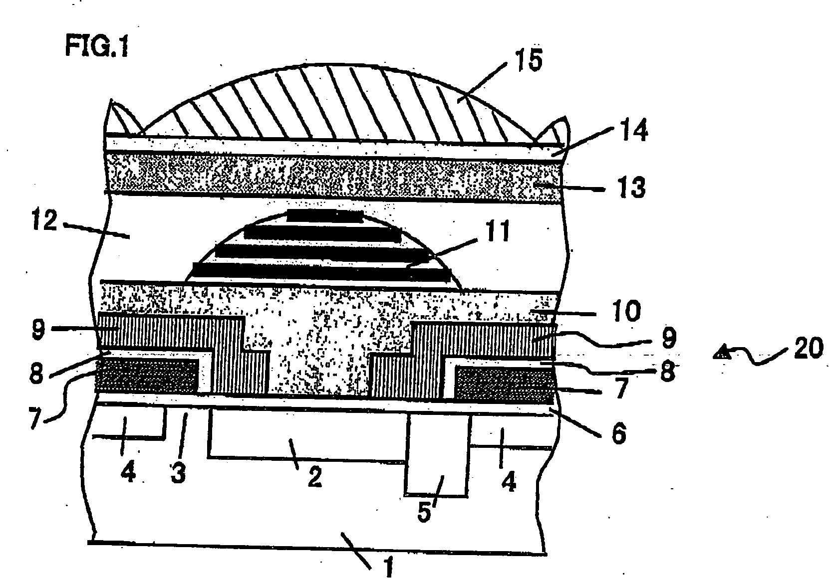
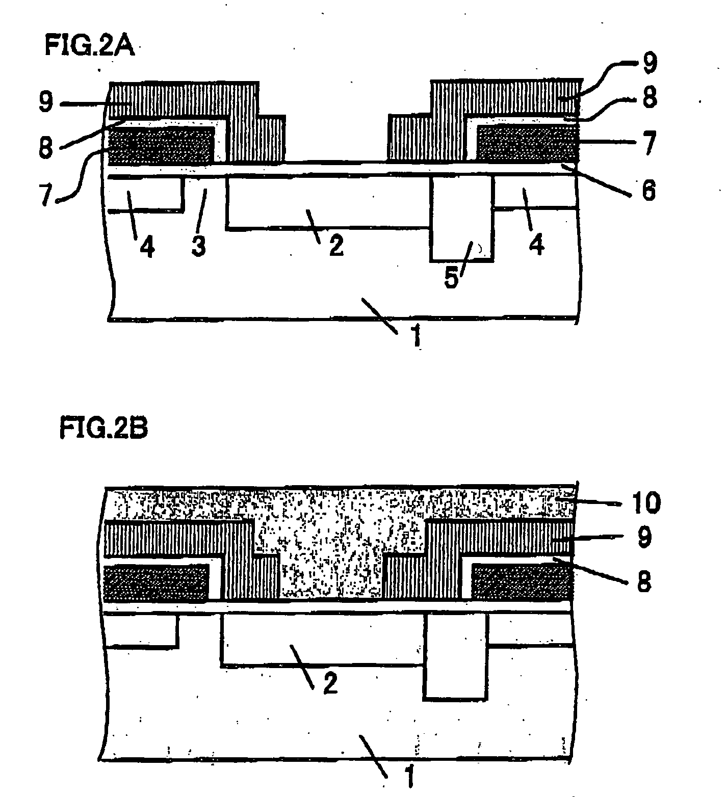
[0059] Hereinafter, embodiments of a semiconductor device and a fabrication method thereof according to the present invention will be described. In the descriptions below, the embodiments of the present invention are embodied as a solid-state image sensing device and a fabrication method thereof. The semiconductor device according to the present invention includes not only a so-called solid-state image sensing device, for example, a CCD image sensor, a CMOS image sensor, a CMD, a charge injection device, a bipolar image sensor, a photoconductive film image sensor, a laminate type CCD image sensor, an infrared image sensor, but also any device which may be used as a light receiving portion or a light emitting portion in various apparatus, for example, a light receiving device produced in a fabrication process for a semiconductor integrated circuit, a light emitting device such as a light emitting diode, a light transmittance control device such as a liquid crystal panel, and the like...


PUM


Abstract

A semiconductor device comprises a photoelectric conversion portion formed on a semiconductor substrate, a first transparent film provided on the photoelectric conversion portion, and an interlayer lens provided on the first transparent film at a position corresponding to the photoelectric conversion portion, in which the interlayer lens has a higher refractive index than the first transparent film, and at least one of upper and lower surfaces of a second transparent film formed with a thin film multilayer structure of two or more types of compounds is formed to have a protruded shape.

Description

[0001] This Nonprovisional application claims priority under 35 U.S.C. §119(a) on Patent Application No.2003-408340 filed in Japan on Dec. 5, 2003, the entire contents of which are hereby incorporated by reference.BACKGROUND OF THE INVENTION [0002] 1. Field of the Invention [0003] The present invention relates to a semiconductor device, such as a solid-state image sensing device which is used in an image input device such as a camera and has an interlayer lens at a position corresponding to a photoelectric conversion portion, and a method for fabricating the same. [0004] 2. Description of the Related Art [0005] Such a solid-state image sensing device includes, for example, a charge coupled device image sensor (hereinafter, simply referred to as CCD), a complementary metal oxide semiconductor (CMOS) image sensor, and the like. These types of solid-state image sensing devices are used in various applications, for example, a digital camera, a video camera, a mobile telephone with an in...

Claims


Application Information

Patent Timeline
Patent Type & Authority Applications(United States)
IPC IPC(8): G02B3/00H01L21/00H01L27/14H01L27/146H01L31/0232H01L31/10
CPCH01L27/14627H01L27/146H01L31/10
Inventor NAKAI, JUNICHIAOKI, TETSURO
Owner SHARP KK
Why Eureka
Try Eureka