Charge pump circuit suitable for low-voltage process

Inactive Publication Date: 2005-07-07
NAT CHIAO TUNG UNIV
View PDF9 Cites 26 Cited by
  • Summary
  • Abstract
  • Description
  • Claims
  • Application Information

AI Technical Summary

Benefits of technology

[0009] It is therefore a primary objective of the claimed invention to provide a charge pump circuit suitable for a low-voltage process that has advantage of high pumping gain. The device is punily affected by the body effect, so the reliability issue of the gate oxide layer in the low-voltage process can be solved.

Problems solved by technology

The charge pump circuit can not only provide the high voltage required for operation of the memory devices but also provide the high voltage for any other purposes.
But the threshold voltage (Vt) of the diode-connected MOSFET is increased with the body effect while voltage of each pumping node is boosted, and that will cause the efficiency of charge pump worse.
The aggravation of charge pump has great influence to the low-voltage source, and will cause the invalidity of the charge pump circuit in memory devices using low-voltage source.
If the voltage source is a typical voltage of manufacture process, such as 1.8V used in the 0.18-μm process of the 40 Å thickness gate oxide layer, most MOSFET in the circuit will exceed the bearable voltage of the gate oxide layer (2*1.8=3.6 V) and lead to the avalanche of the gate oxide layer and the invalidity of the device.

Method used


Image

  • Charge pump circuit suitable for low-voltage process
  • Charge pump circuit suitable for low-voltage process
  • Charge pump circuit suitable for low-voltage process

Examples


Embodiment Construction

[0029] The charge pump circuit is popularly used in the integrated circuits, such as in the memory IC, the analog or digital IC and the LCD drive IC. With the progression of process, the voltage tolerance of devices is getting smaller, and the present invention discloses a charge pump circuit suitable for a low-voltage process that has high pumping gain and no exceeding voltage on the gate oxide layer.

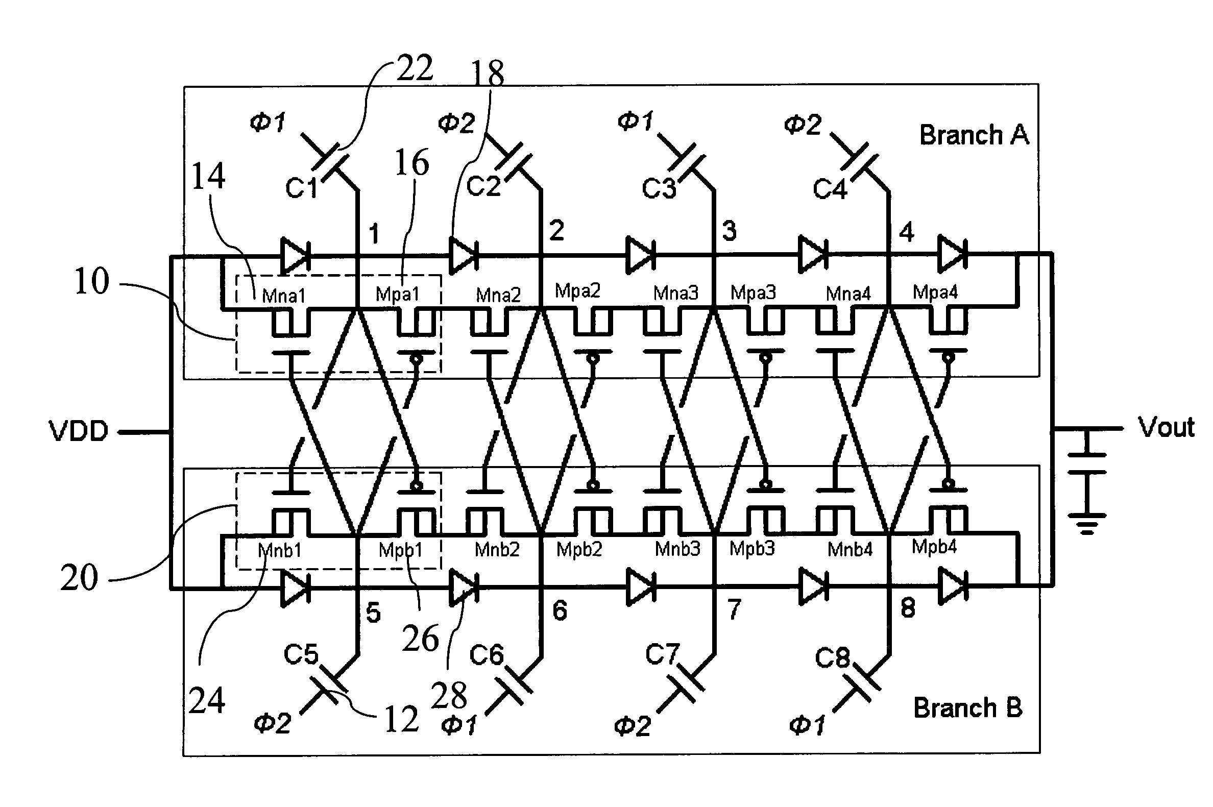
[0030] The claimed charge pump circuit is composed of a plurality of stages (1-stage to n-stage) of voltage amplifying circuits connected each other, and the operation of two adjacent stages of voltage amplifying circuits is controlled by two opposite timing signals. The embodiment in FIG. 3(a) uses a 4-stage voltage amplifying circuit to explain the present invention.

[0031] As shown in FIG. 3(a), each stage of the voltage amplifying circuit comprises a coupled pair of a first complementary MOS (CMOS) transistor 10 and a second CMOS transistor 20. The first CMOS transistor 10 is conn...


PUM


Abstract

The present invention discloses a charge pump circuit suitable for a low-voltage process. The charge pump circuit is composed of stages of the voltage amplifying circuits connected each other, and the operation of two adjacent stages of voltage amplifying circuit is controlled by two opposite set of the timing signals. Each stage of the voltage amplifying circuit has a coupled pair of a first complementary MOS (CMOS) transistor and a second CMOS transistor switching in accordance with a timing signal and an inverse timing signal inputted into the first and second capacitors. Then, two diode devices guide charges to next stage, and a voltage higher than the integrated circuit voltage source is outputted. The present invention has advantage of high pumping gain, and the reliability issue of the gate oxide layer in the low-voltage process can be also solved.

Description

BACKGROUND OF INVENTION [0001] 1. Field of the Invention [0002] The invention relates to a charge pump circuit, and more particularly, to a charge pump circuit suitable for a low-voltage process and having a high pumping gain. [0003] 2. Description of the Prior Art [0004] When using the general volatile memory devices, such as dynamic random access memory (DRAM) or static random access memory (SRAM), the stored data will be removed after turning the power off. If we want to keep the data after turning the power off, we should use the non-volatile memory devices, such as read-only memory (ROM), programmable read-only memory (PROM), erasable programmable read-only memory (EPROM), electrically erasable programmable read-only memory (EEPROM) and flash memory (Flash). [0005] The EEPROM or Flash needs a charge pump circuit to provide a voltage higher than the integrated circuit voltage source to perform the program or erase procedure. The charge pump circuit can not only provide the high ...

Claims


Application Information

Patent Timeline
IPC IPC(8): G05F3/02G11C16/06H02M3/07
CPCH02M3/073H02M2003/077H02M2003/075H02M3/075H02M3/077
Inventor KER, MING-DOUTSAI, CHIA-SHENG
Owner NAT CHIAO TUNG UNIV
Why Eureka
Try Eureka