Charge pump device and operating method thereof

a technology of a pump device and a discharge pump, which is applied in the direction of electric variable regulation, process and machine control, instruments, etc., can solve the problems of reducing the conduction performance (charge transfer efficiency) of the transistor, unable to provide an efficient load current, and inferior charge transfer efficiency, etc., to achieve high negative level, eliminate the body effect, and high pumping gain

Inactive Publication Date: 2009-03-12
YIELD MICROELECTRONICS CORP
View PDF2 Cites 1 Cited by
  • Summary
  • Abstract
  • Description
  • Claims
  • Application Information

AI Technical Summary

Benefits of technology

[0011]The primary object of the present invention is to provide a charge pump device and an operating method thereof to eliminate the body effect for providing an output voltage with a high negative level and also have the advantage of a high pumping gain.

Problems solved by technology

An obvious body effect or a raised threshold voltage of a transistor will reduce the conduction performance (charge transfer efficiency) of the transistor.
Higher threshold voltages of the PMOS transistors P0˜P4 in FIG. 1(a) means more PMOS transistors are cascaded to cause an inferior charge transfer efficiency so as to be unable to provide an efficient load current.
Therefore, the charge pump device 20 also has an obvious body effect or raised threshold voltages of transistor, hence lowering the conduction performance (charge transfer efficiency) of transistor.

Method used


Image

  • Charge pump device and operating method thereof
  • Charge pump device and operating method thereof
  • Charge pump device and operating method thereof

Examples


Embodiment Construction

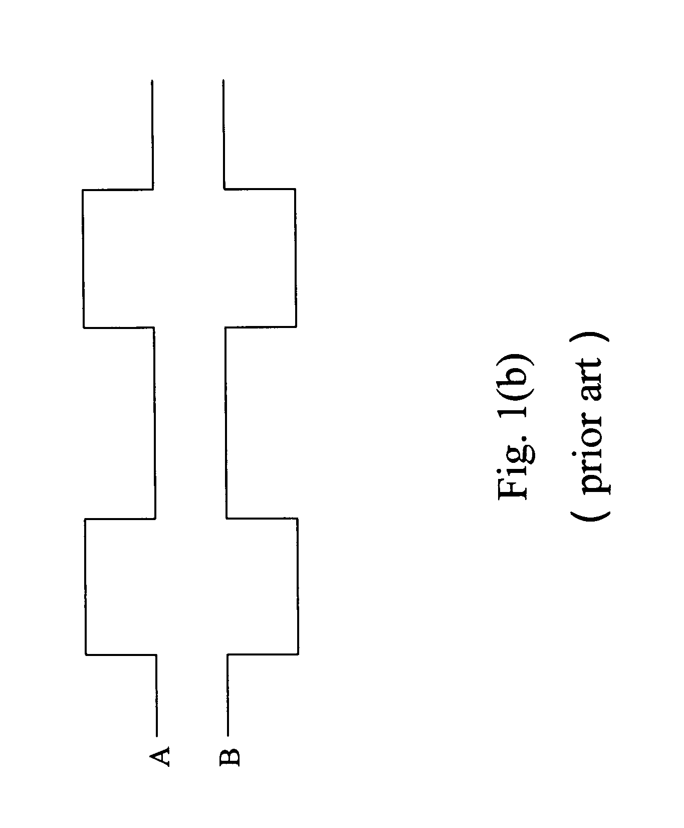
[0024]FIG. 3(a) is a diagram of a charge pump device according to the first embodiment of the present invention. Please also refer to FIG. 3(b). A charge pump device 30 is composed of a first-stage charge transfer unit 31, a second-stage charge transfer unit 32 and an output unit 33 that are cascaded between an input node Nin and an output node Nout. In order to get a negative voltage, the voltage level of the power source connected to the input node Nin is at the ground level, and the output node is used to provide the output voltage.

[0025]Each stage of charge transfer units comprises a first node X (X′), a second node Y (Y′), a first circuit 34 (35) connected between the two nodes, and a first capacitor C1 (C2) connected to the second node Y (Y′). The first circuit 34 (35) includes a fourth node Z (Z′), a fifth node W (W′), an eighth node NW1 (NW2), a first transistor M30 (M34), a second transistor M31 (M35), a third transistor M32 (M36), a fourth transistor M33 (M37), and a first...


PUM


Abstract

A charge pump device and an operating method thereof are proposed. The charge pump device is composed of a plurality of stages of charge transfer units and an output unit that are cascaded together. Each stage of the charge transfer units includes a first node for input, a second node for output, a first circuit and a first capacitor. The first node or the second node is biased at a bias provided for the first circuit. Thereby, the first capacitors of the odd-numbered stage and the even-numbered stage of charge transfer units can respectively receive two clock signals that are mutually opposite in phase for complementary switching operating. Collocated with the switching of the output unit, an output voltage with a high negative level can be generated.

Description

BACKGROUND OF THE INVENTION[0001]1. Field of the Invention[0002]The present invention relates to a charge pump technology and, more particularly, to a charge pump device capable of eliminating the body effect and having a high pumping gain and an operating method thereof.[0003]2. Description of Related Art[0004]Negative voltages are required for general flash memories or electrically erasable programmable read only memories (EEPROM) to generate a sufficient relative potential difference for data erase or data programming function.[0005]FIG. 1 shows a prior art charge pump device 10, which makes use of cascaded PMOS transistors to transfer charges in the load capacitor of the output node. The input node of this charge pump device 10 is grounded. The drain of each of the PMOS transistors P0˜P4 is connected to the gate thereof. The PMOS transistors are cascaded together in the so-called diode-connected manner. All the substrates of the PMOS transistors P0˜P4 are biased at the voltage l...

Claims


Application Information

Patent Timeline
Patent Type & Authority Applications(United States)
IPC IPC(8): G05F3/02
CPCH02M2003/078H02M3/073H02M3/078
Inventor LIN, HSIN CHANGWU, CHENG YING
Owner YIELD MICROELECTRONICS CORP
Why Eureka
Try Eureka