
Semiconductor on insulator vertical transistor fabrication and doping process

Inactive Publication Date: 2005-06-23
APPLIED MATERIALS INC
View PDF99 Cites 174 Cited by
  • Summary
  • Abstract
  • Description
  • Claims
  • Application Information

AI Technical Summary

Benefits of technology

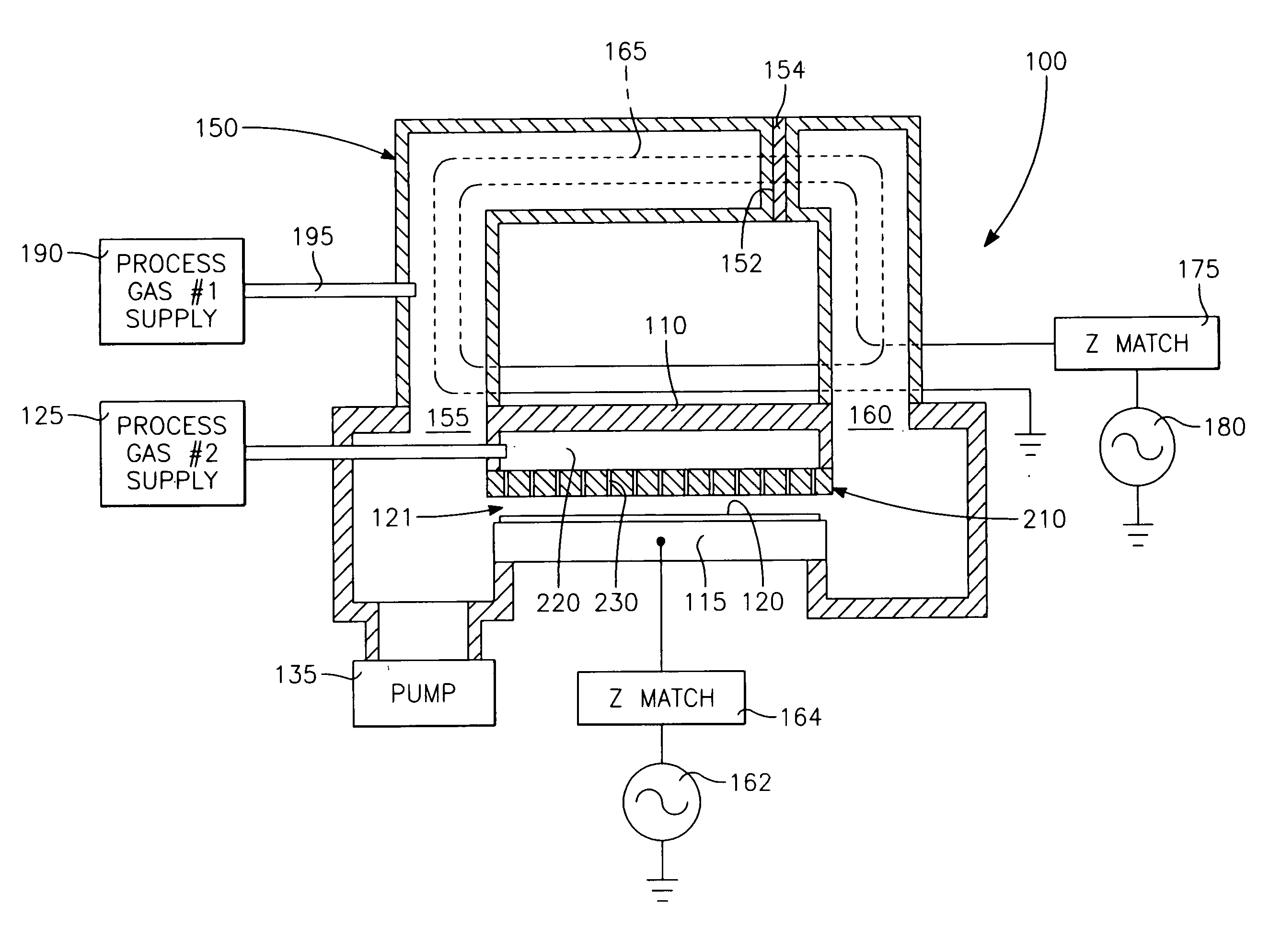
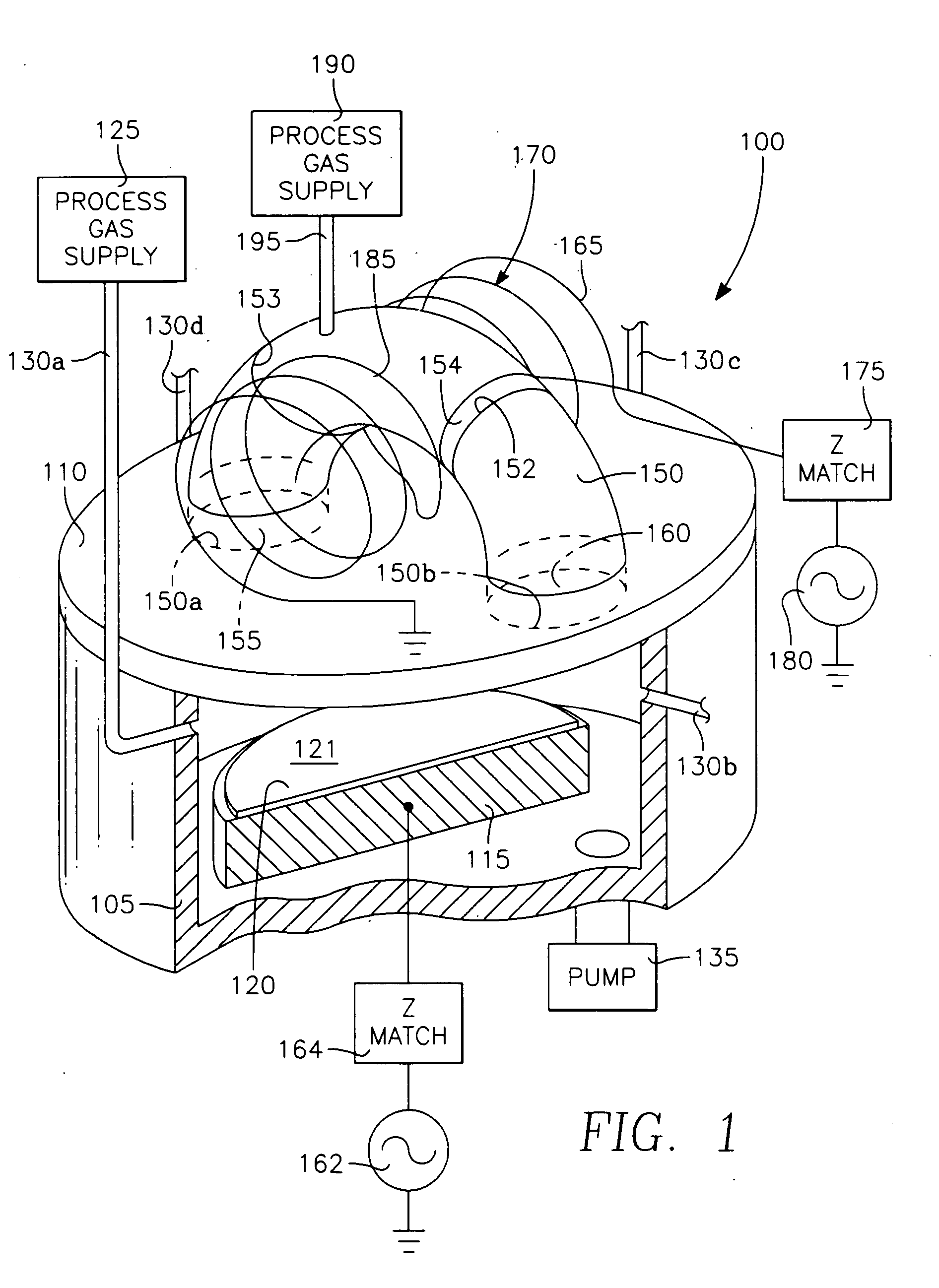
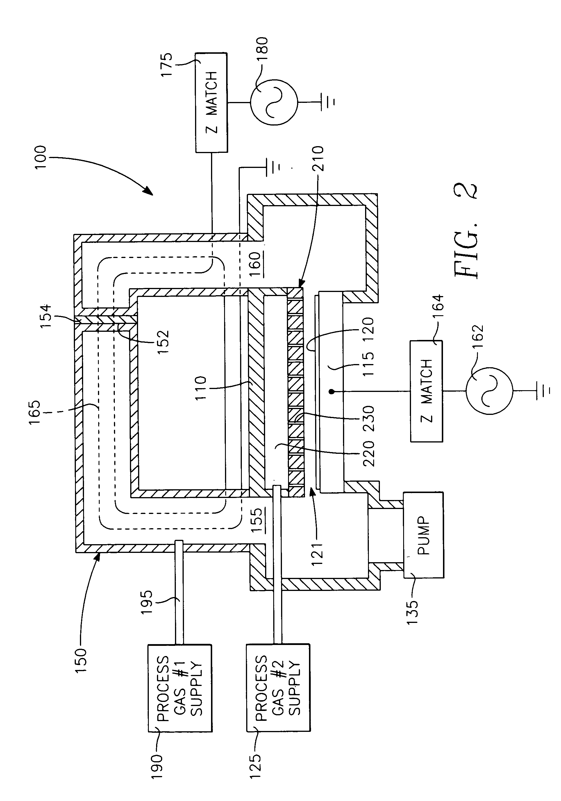
[0005] A process is disclosed for fabricating a vertical transistor on a semiconductor-on-insulator wafer consisting of an underlying substrate, an intermediate insulator layer and a top crystalline semiconductor active layer. The process includes sculpting from the active layer a 3-dimensional source-channel-drain structure having horizontal and vertical surfaces and comprising a channel with a source and drain at either end of the channel, and forming a conformal thin gate oxide layer over a section of the channel. A 3-dimensional gate structure is formed over of said thin gate oxide layer. While supporting the wafer in a torroidal source plasma reactor chamber having at least one external reentrant

Problems solved by technology

Planar transistor structures formed in an SOI island are still limited in their performance by the presence of a PN junction between the source or drain and the surrounding semiconductor material.
However, this technique is not ideal because nearby or neighboring vertical transistor structures may shadow some of the surfaces during ion implantation.

Method used


Image

  • Semiconductor on insulator vertical transistor fabrication and doping process
  • Semiconductor on insulator vertical transistor fabrication and doping process
  • Semiconductor on insulator vertical transistor fabrication and doping process

Examples


working examples

[0324] A principal application of a PIII reactor is the formation of PN junctions in semiconductor crystals. FIGS. 109 and 110 illustrate different stages in the deposition of dopant impurities in the fabrication of a P-channel metal oxide semiconductor field effect transistor (MOSFET). Referring first to FIG. 109, a region 9960 of a semiconductor (e.g., silicon) wafer may be doped with an N-type conductivity impurity, such as arsenic or phosphorus, the region 9960 being labeled “n” in the drawing of FIG. 109 to denote its conductivity type. A very thin silicon dioxide layer 9962 is deposited on the surface of the wafer including over n-type region 9960. A polycrystalline silicon gate 9964 is formed over the thin oxide layer 9962 from a blanket polysilicon layer that has been doped with boron in the PIII reactor. After formation of the gate 9964, p-type dopant is implanted in the PIII reactor to form source and drain extensions 9972 and 9973. Spacer layers 9966 of a dielectric mater...


PUM


Abstract

A process for conformally doping through the vertical and horizontal surfaces of a 3-dimensional vertical transistor in a semiconductor-on-insulator structure employs an RF oscillating torroidal plasma current to perform either conformal ion implantation, or conformal deposition of a dopant-containing film which can then be heated to drive the dopants into the transistor. Some embodiments employ both conformal ion implantation and conformal deposition of dopant containing films, and in those embodiments in which the dopant containing film is a pure dopant, the ion implantation and film deposition can be performed simultaneously.

Description

CROSS-REFERENCE TO RELATED APPLICATIONS [0001] This application is a continuation-in-part of U.S. application Ser. No. 10 / 838,052 filed May 3, 2004 entitled LOW TEMPERATURE CVD PROCESS WITH CONFORMALITY, STRESS AND COMPOSITION by Hiroji Hanawa, et al., which is a continuation-in-part of U.S. patent application Ser. No. 10 / 786,410 filed Feb. 24, 2004 entitled FABRICATION OF SILICON-ON-INSULATOR STRUCTURE USING PLASMA IMMERSION ION IMPLANTATION by Dan Maydan et al., which is a continuation-in-part of U.S. patent application Ser. No. 10 / 646,533 filed Aug. 22, 2003 entitled PLASMA IMMERSION ION IMPLANTATION PROCESS USING A PLASMA SOURCE HAVING LOW DISSOCIATION AND LOW MINIMUM PLASMA VOLTAGE by Kenneth Collins et al., which is a continuation-in-part of U.S. patent application Ser. No. 10 / 164,327 filed Jun. 5, 2003 entitled EXTERNALLY EXCITED TORROIDAL PLASMA SOURCE WITH MAGNETIC CONTROL OF ION DISTRIBUTION by Kenneth Collins et al., which is a continuation-in-part of U.S. patent applicat...

Claims


Application Information

Patent Timeline
IPC IPC(8): H01J37/32
CPCH01J37/321H01L29/66795H01L29/78618H01L29/7843H01L29/785H01L29/66803
Inventor AL-BAYATI, AMIRCOLLINS, KENNETH S.HANAWA, HIROJIRAMASWAMY, KARTIKGALLO, BIAGIONGUYEN, ANDREW
Owner APPLIED MATERIALS INC
Learn More