Laser module
a laser module and module technology, applied in the direction of lasers, optical resonator shape and construction, semiconductor lasers, etc., can solve the problems of insufficient monochromatic characteristics, increased data traffic, and difficult to amplify wavelength-multiplexed signal light as designed
- Summary
- Abstract
- Description
- Claims
- Application Information
AI Technical Summary
Benefits of technology
Problems solved by technology
Method used
Image
Examples
first embodiment
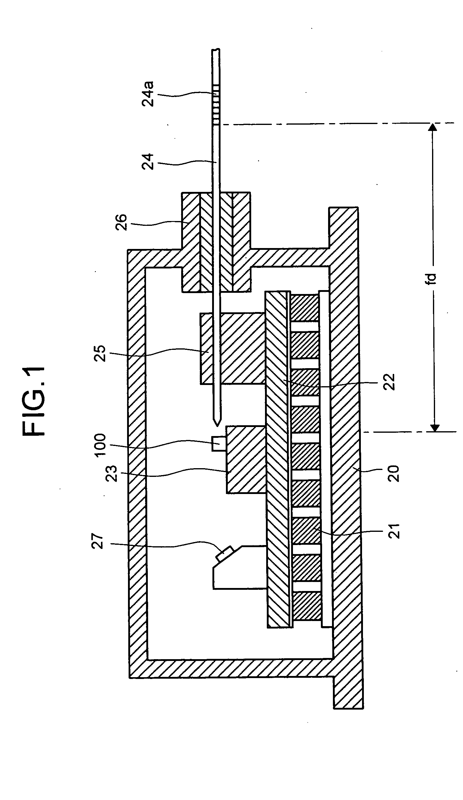
[0101] As has been described above, in the laser module including at lease the semiconductor laser element 100 having the DCH structure and the FBG 24a, by satisfying a condition in which a total RIN in a high frequency range is equal to or not less than a predetermined value, a coherence-collapse phenomenon and sufficient monochromatic characteristic can be simultaneously achieved, thereby realizing sufficiently-stable light outputs in low frequencies. Furthermore, laser modules under the same conditions can have a characteristic satisfying an SMSR even with any polarized state of returned light occurring due to a kink of the optical fiber or the like, that is, even with fluctuations in threshold current that occur accordingly.
[0102] In the description of the first embodiment above, measurement results have been shown when the cavity length fd between the FBG 24a and the semiconductor laser element 100 is assumed to be 1 meter. Therefore, if the cavity length fd has a different va...
second embodiment
[0104]FIG. 16 is a perspective view of a laser module according to the present invention having an SCH structure. As shown in FIG. 16, a semiconductor laser element 200 included in the laser module 200 has an upper portion being shaped like a ridge waveguide and, as a whole, having a predetermined cavity length L. On a substrate 10 made of n-GaAs, a lower clad layer 11A made of n-AlGaAs is formed, on which a layer structure E, which will be described further below, is further formed. On the rear surface of the substrate 10, an n-type electrode 12A is formed. On the upper surface of the layer structure E, a p-type electrode 12B is formed via a protective film 13 made of silicon nitride (SiNx) or the like.
[0105] The layer structure E includes an active layer 14 having a quantum well structure including three well layers 14A0, 14A1, and 14A2 made of InGaAs and four barrier layers 14B1, 14B2, 14B3, and 14B4 made of GaAsP and disposed on both sides of each well layer. On a side of each o...
PUM
 Abstract
Description
Claims
Application Information
 - R&D
- Intellectual Property
- Life Sciences
- Materials
- Tech Scout
- Unparalleled Data Quality
- Higher Quality Content
- 60% Fewer Hallucinations
Browse by: Latest US Patents, China's latest patents, Technical Efficacy Thesaurus, Application Domain, Technology Topic, Popular Technical Reports.
© 2025 PatSnap. All rights reserved.Legal|Privacy policy|Modern Slavery Act Transparency Statement|Sitemap|About US| Contact US: help@patsnap.com


