Method of fabricating a MOSFET device
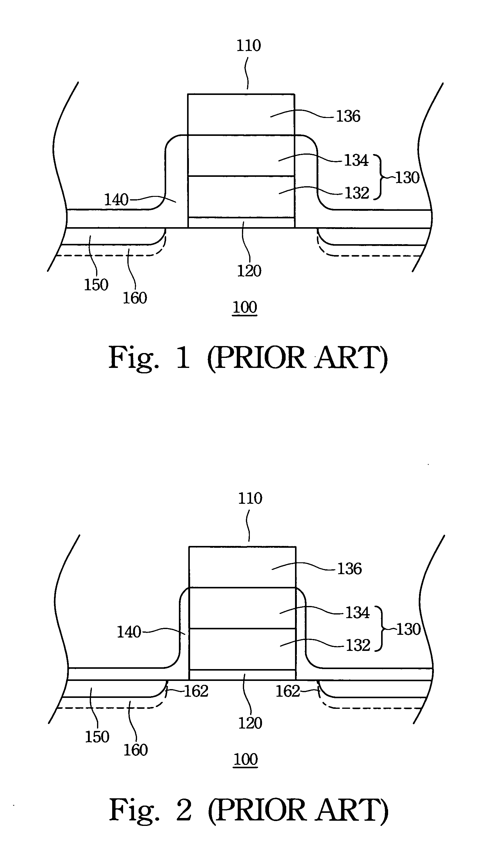
a technology of metal oxidesemiconductor and field effect transistor, which is applied in the direction of semiconductor devices, transistors, electrical appliances, etc., can solve the problems of sub-threshold leakage, depletion regions at these junctions, and unsatisfactory effects when channel length is reduced to a certain degree, so as to achieve effective solution the effect of problems
- Summary
- Abstract
- Description
- Claims
- Application Information
AI Technical Summary
Benefits of technology
Problems solved by technology
Method used
Image
Examples
first embodiment
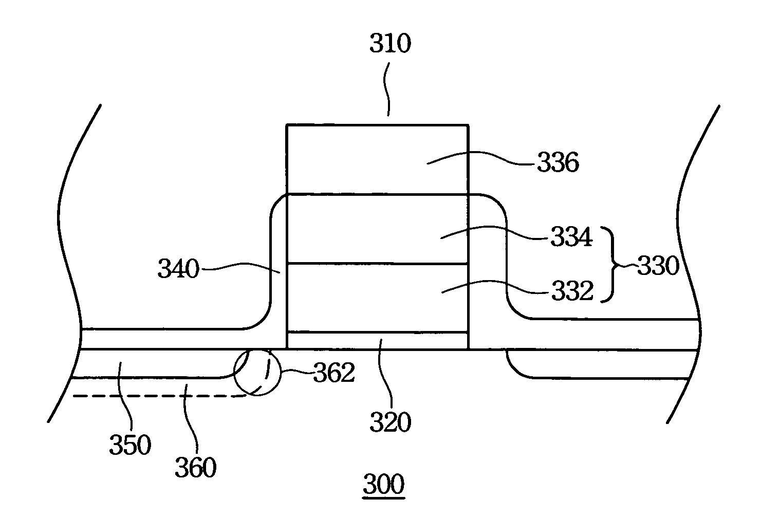
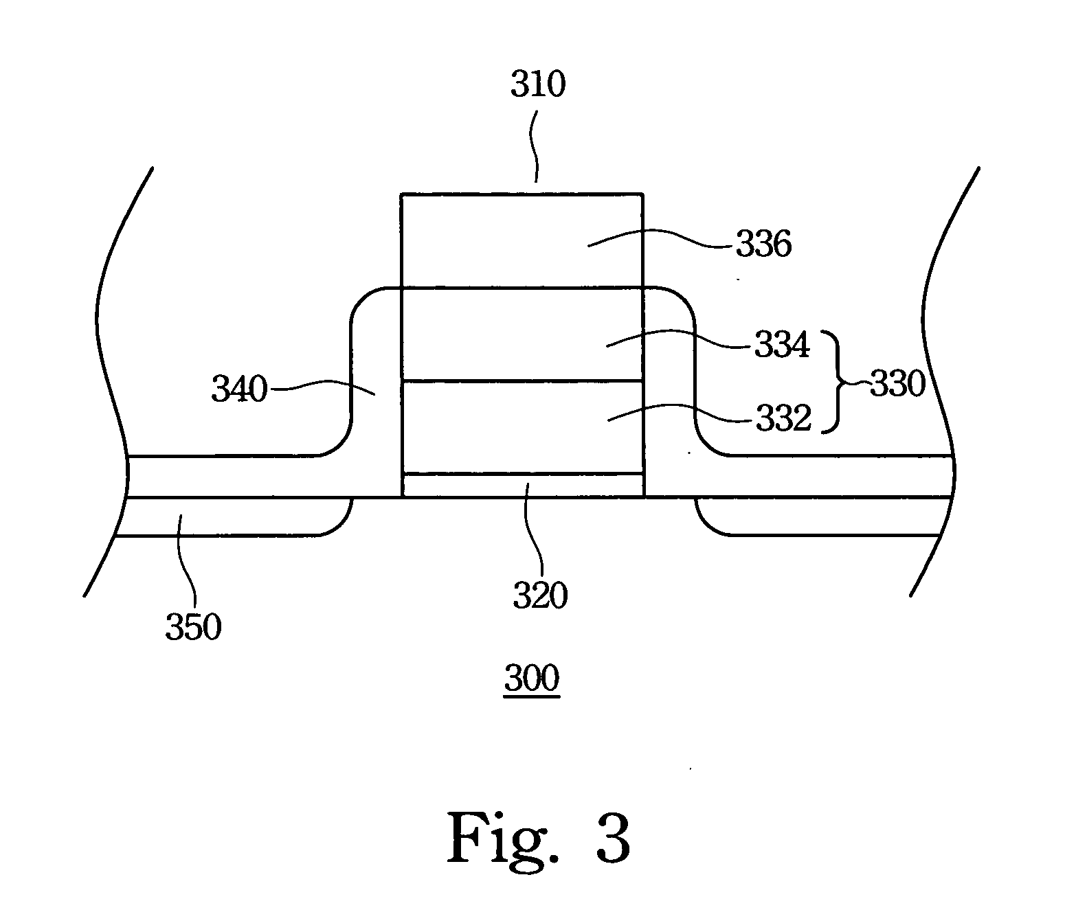
[0022] A first embodiment of the present invention is described here. FIG. 3 illustrates a cross section of an N-channel MOSFET structure having source and drain regions according to an embodiment of the invention. FIG. 4A illustrates a cross section of the N-channel MOSFET structure in FIG. 3 after etching the liner at two sides of the gate and performing the halo implantation. In the following description, the same reference numerals are utilized for substantially similar elements in FIGS. 3, 4A and 4B, for the purpose of clarity. However, it will be apparent to one skilled in the art, for example, that some of the “like” elements may not actually be substantially similar or identical, after various steps in the semiconductor process.
[0023] The process of forming the structure in FIG. 3 is described as follows. A gate dielectric layer 320 is initially formed, using, for example, thermal oxidation, on a substrate 300. The substrate 300 is, for example, a P-type semiconductor mater...
second embodiment
[0027] A second embodiment of the present invention is described here. FIG. 4B illustrates a cross section of the N-channel MOSFET structure in FIG. 3 after etching the liner and performing the halo implantation at one side of the gate. With reference to FIG. 4B, after completing the structure in FIG. 3, a mask layer (not shown), for example a photoresist layer, is formed to cover a side of the gate 310. Next, part of the liner 340 at another side of the gate 310 is etched to reduce its thickness. A second-type ion implantation is then performed, using the gate 310 and the etched portion of the liner 340 as a mask, to form a P-type halo region 360 surrounding one of the source / drain regions 350 adjacent to the etching side in the substrate 300. The second-type ion is, for example, boron ions for a P-type material. Now the structure in FIG. 4B has been completed.
[0028] From the above preferred embodiment of the invention, advantages of using the invention include the following. As s...
PUM
 Abstract
Description
Claims
Application Information
 - R&D
- Intellectual Property
- Life Sciences
- Materials
- Tech Scout
- Unparalleled Data Quality
- Higher Quality Content
- 60% Fewer Hallucinations
Browse by: Latest US Patents, China's latest patents, Technical Efficacy Thesaurus, Application Domain, Technology Topic, Popular Technical Reports.
© 2025 PatSnap. All rights reserved.Legal|Privacy policy|Modern Slavery Act Transparency Statement|Sitemap|About US| Contact US: help@patsnap.com


