
Forming a semiconductor structure in manufacturing a semiconductor device using one or more epitaxial growth processes

a technology of epitaxial growth and semiconductor structure, which is applied in the field of semiconductor structure formation in the manufacture of semiconductor devices, can solve the problems of unsatisfactory stress in the semiconductor structure, and achieve the effect of reducing the disadvantages and eliminating the problems of previous techniques for forming semiconductor structure in the manufacturing of semiconductor devices

Inactive Publication Date: 2005-05-19
TEXAS INSTR INC
View PDF9 Cites 125 Cited by
  • Summary
  • Abstract
  • Description
  • Claims
  • Application Information

AI Technical Summary

Benefits of technology

[0005] According to the present invention, disadvantages and problems associated with previous techniques for forming semiconductor structures in manufacturing semiconductor devices may be reduced or eliminated.
[0008] Particular embodiments of the present invention may provide one or more technical advantages. For example, forming a semiconductor structure according to the present invention may change the production paradigm by reducing or eliminating the need for the implant and anneal steps. In certain embodiments, etching an oxide layer deposited on a substrate layer to form one or more isolation regions and epitaxially growing a substrate material on an epitaxial growth surface defined by the isolation regions may improve transistor performance because epitaxial growth may be a relatively controlled process. In certain embodiments, this may reduce or eliminate an STI step-height problem resulting from previous techniques for forming isolation regions to define active regions. Additionally, in certain embodiments, the relatively controlled epitaxial growth process may be preferable when forming smaller semiconductor devices because the added control may improve scaling. Furthermore, in certain embodiments, previous STI etch and fill techniques for forming the isolation regions may involve etching a trench for each isolation region and introducing a liner oxide layer in each of the trenches, which may lead to undesirable stress in the semiconductor structure. In certain embodiments, the liner oxide layer may not be introduced, which may reduce or eliminate the undesirable stress.
[0009] In certain embodiments, one or more dopant materials may be introduced into the epitaxially-grown substrate material as the substrate material is epitaxially grown, which may eliminate the need for the relatively imprecise implant and anneal steps. In certain embodiments, reducing or eliminating the need to introduce dopants using the implant step may reduce or eliminate problems related to diffusion of dopant material during the anneal step. For example, in certain embodiments, epitaxial growth allows the dopant material to be relatively precisely introduced into the substrate material. In certain embodiments, this, along with the elimination of the need for the implant and anneal steps, may provide more freedom to tailor the doping gradient as desired. For example, in certain embodiments, introducing the dopant material into the substrate material as it is epitaxially grown may allow the doping gradient to be made steeper. In certain embodiments, the epitaxial growth process may provide a relatively controlled process for introducing dopant material into the substrate material. In certain embodiments, the epitaxial growth process may be a substantially self-aligned process when introducing dopant material into the substrate material, whereas the implant and anneal steps may suffer from misalignment. Additionally, in certain embodiments, the dopant material may include germanium (Ge). In these embodiments, the ability to relatively precisely introduce Ge in the epitaxially-grown substrate material may improve stress-engineering of the semiconductor structure.
[0010] In certain embodiments, forming a transistor in the semiconductor structure using one or more substantially vertical isolation layers formed on each side of a gate of the transistor and one or more epitaxially-grown extenders grown on each side of the gate and adapted to serve as a source and drain of the transistor may improve transistor performance. For example, in certain embodiments, reducing or eliminating the need for the implant or anneal process for introducing a dopant material into the active region to form the source and drain of the transistor may reduce or eliminate problems associated with diffusion of the dopant material. Furthermore, in certain embodiments, using the epitaxially-grown extenders to form the source and the drain of the transistor above the substrate surface may provide a better geometry for the transistor, which may improve transistor performance.

Problems solved by technology

Furthermore, in certain embodiments, previous STI etch and fill techniques for forming the isolation regions may involve etching a trench for each isolation region and introducing a liner oxide layer in each of the trenches, which may lead to undesirable stress in the semiconductor structure.

Method used


Image

  • Forming a semiconductor structure in manufacturing a semiconductor device using one or more epitaxial growth processes
  • Forming a semiconductor structure in manufacturing a semiconductor device using one or more epitaxial growth processes
  • Forming a semiconductor structure in manufacturing a semiconductor device using one or more epitaxial growth processes

Examples


Embodiment Construction

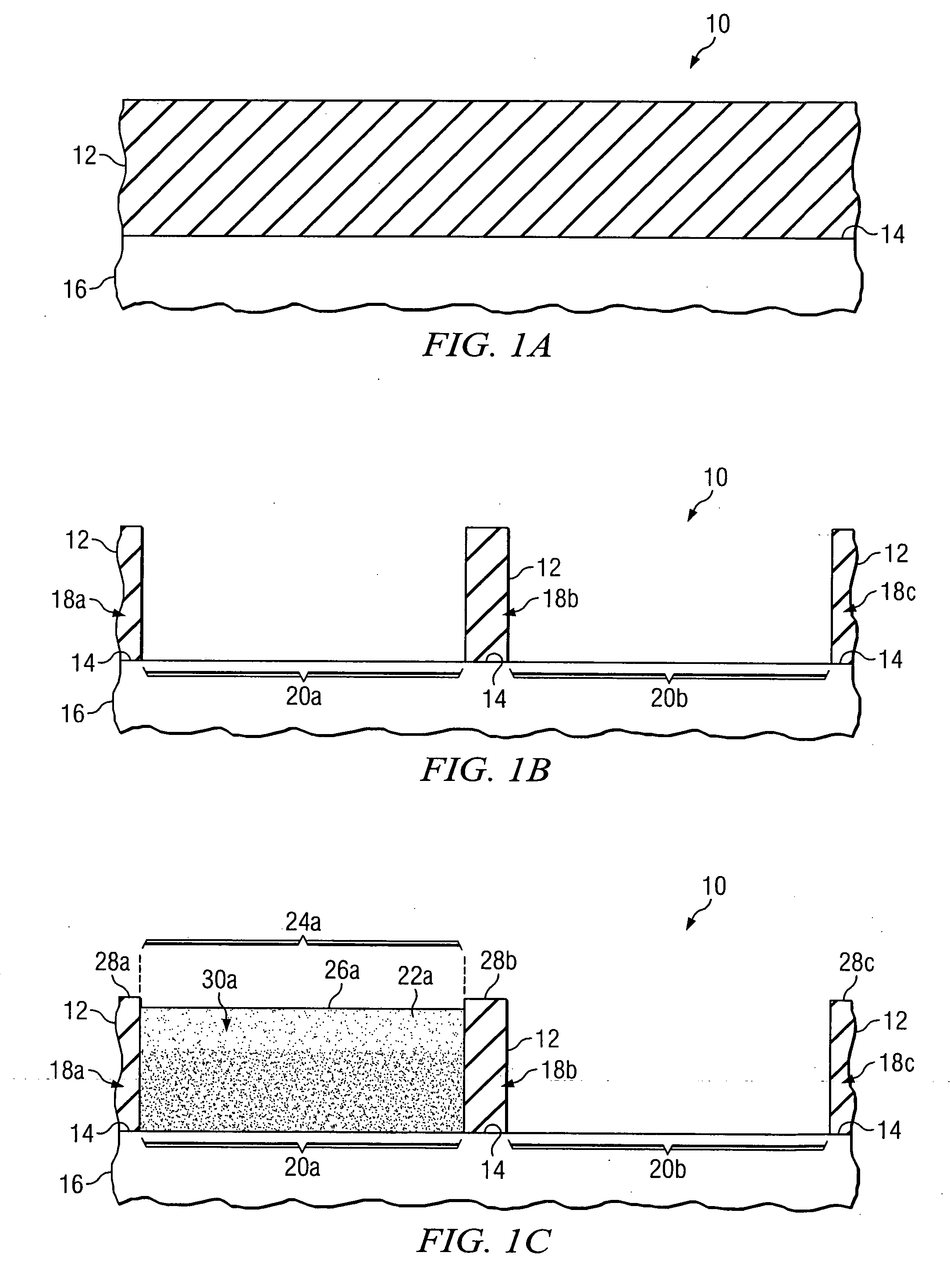
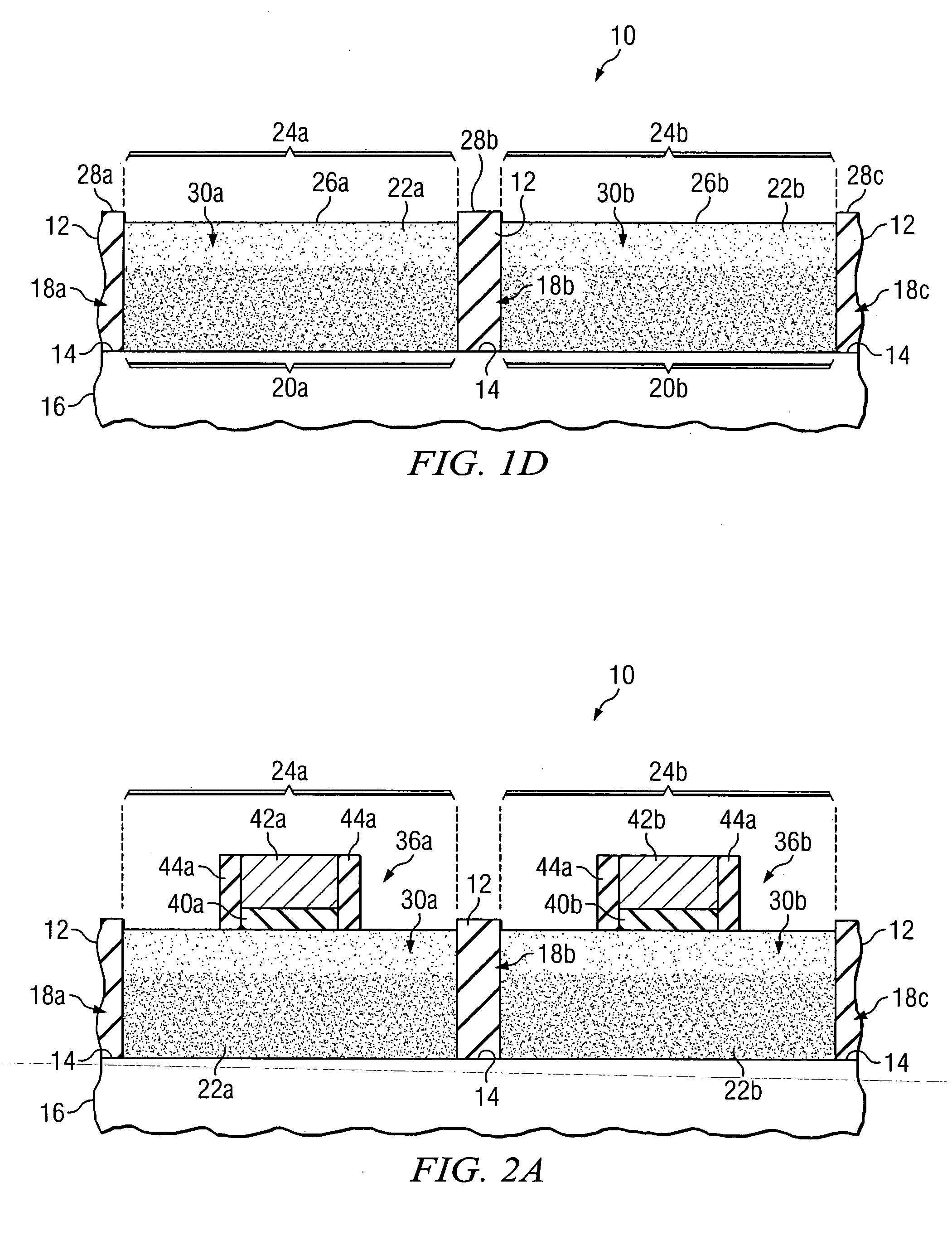
[0015]FIGS. 1A-1D illustrate an example process for forming a semiconductor structure 10 in manufacturing a semiconductor device, the semiconductor structure 10 formed using one or more epitaxial growth processes and having one or more isolation regions separating one or more active regions. In one embodiment, the semiconductor device includes a complementary metal oxide semiconductor (CMOS) device, such as a p-channel metal oxide semiconductor (PMOS) device or n-channel metal oxide semiconductor (NMOS) device.

[0016] As shown in FIG. 1A, an oxide layer 12 may be provided on a surface 14 of a silicon or other substrate layer 16. While surface 14 is illustrated as being substantially flat, surface 14 may have any suitable profile according to particular needs or manufacturing tolerances, for example. Oxide layer 12 may be grown on surface 14 of substrate layer 16 using any suitable technique, deposited on surface 14 of substrate layer 16 using any suitable technique, or otherwise pro...


PUM


Abstract

In one embodiment, a semiconductor structure used in manufacturing a semiconductor device includes a substrate layer. The structure also includes first and second isolation regions formed by etching an oxide layer provided on the substrate layer to define an epitaxial growth surface of the substrate layer for epitaxial growth of a substrate material on the epitaxial growth surface between the first and second isolation regions. The structure also includes an active region that includes the epitaxially-grown substrate material between the first and second isolation regions, the active region formed by epitaxially growing the substrate material on the epitaxial growth surface of the substrate layer.

Description

TECHNICAL FIELD [0001] This invention relates generally to semiconductor structures, and more particularly to forming a semiconductor structure in manufacturing a semiconductor device using one or more epitaxial growth processes. BACKGROUND [0002] Integrated circuit fabrication often includes forming one or more isolation regions to define one or more active regions on a silicon or other substrate of a semiconductor structure. One way to form an isolation region is to form one or more trenches in the substrate using one or more etching processes while masking the substrate over what is to be the active region. As an example, this process may be referred to as shallow trench isolation (STI). Subsequent to formation, a liner oxide layer may be formed in the trenches and the trenches may be filled with a fill oxide to form the isolation regions. The etching processes for forming the isolation regions may lead to problems that may degrade transistor performance. These problems may inclu...

Claims


Application Information

Patent Timeline
Patent Type & Authority Applications(United States)
IPC IPC(8): H01L21/8238H01L27/00
CPCH01L21/823878H01L21/823807
Inventor WASSHUBER, CHRISTOPH A.
Owner TEXAS INSTR INC
Learn More