
Method of fabricating a thin film transistor and manufacturing equipment

a technology of thin film transistor and manufacturing equipment, which is applied in the direction of transistors, chemical vapor deposition coatings, coatings, etc., can solve the problems of deteriorating interface properties between the bcb gate-insulating layer and the active layer, contaminated bcb film, and breakage of the gate-insulating layer, etc., to achieve the effect of improving the interface property

Inactive Publication Date: 2005-04-28
LG DISPLAY CO LTD
View PDF5 Cites 16 Cited by
  • Summary
  • Abstract
  • Description
  • Claims
  • Application Information

AI Technical Summary

Benefits of technology

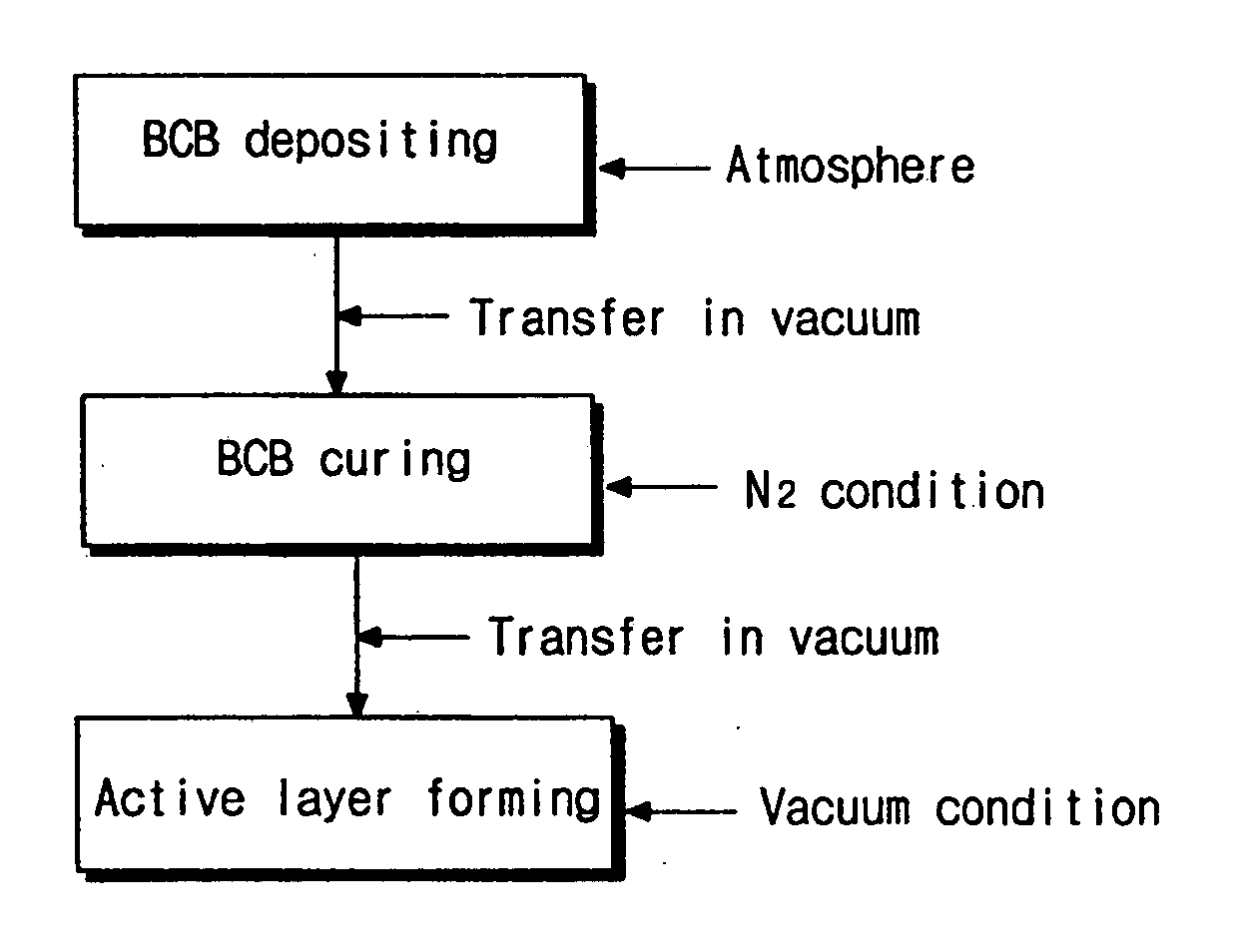
The present invention provides a method and apparatus for fabricating a thin film transistor with an improved interface property using an organic insulating layer. The method includes curing the organic insulating layer in a vacuum and transferring the substrate to a second chamber for forming a silicon layer without breaking the vacuum. The apparatus includes a preparation chamber for providing a vacuum condition during transfer of the substrate between different chambers. The invention also provides a method of making a liquid crystal display device with a thin film transistor and a method of forming a pixel electrode. The technical effects of the invention include improved interface property of the thin film transistor, simplified fabrication process, and improved display quality of the liquid crystal display device.

Problems solved by technology

However, pure aluminum often produces hillocks that can cause defects.
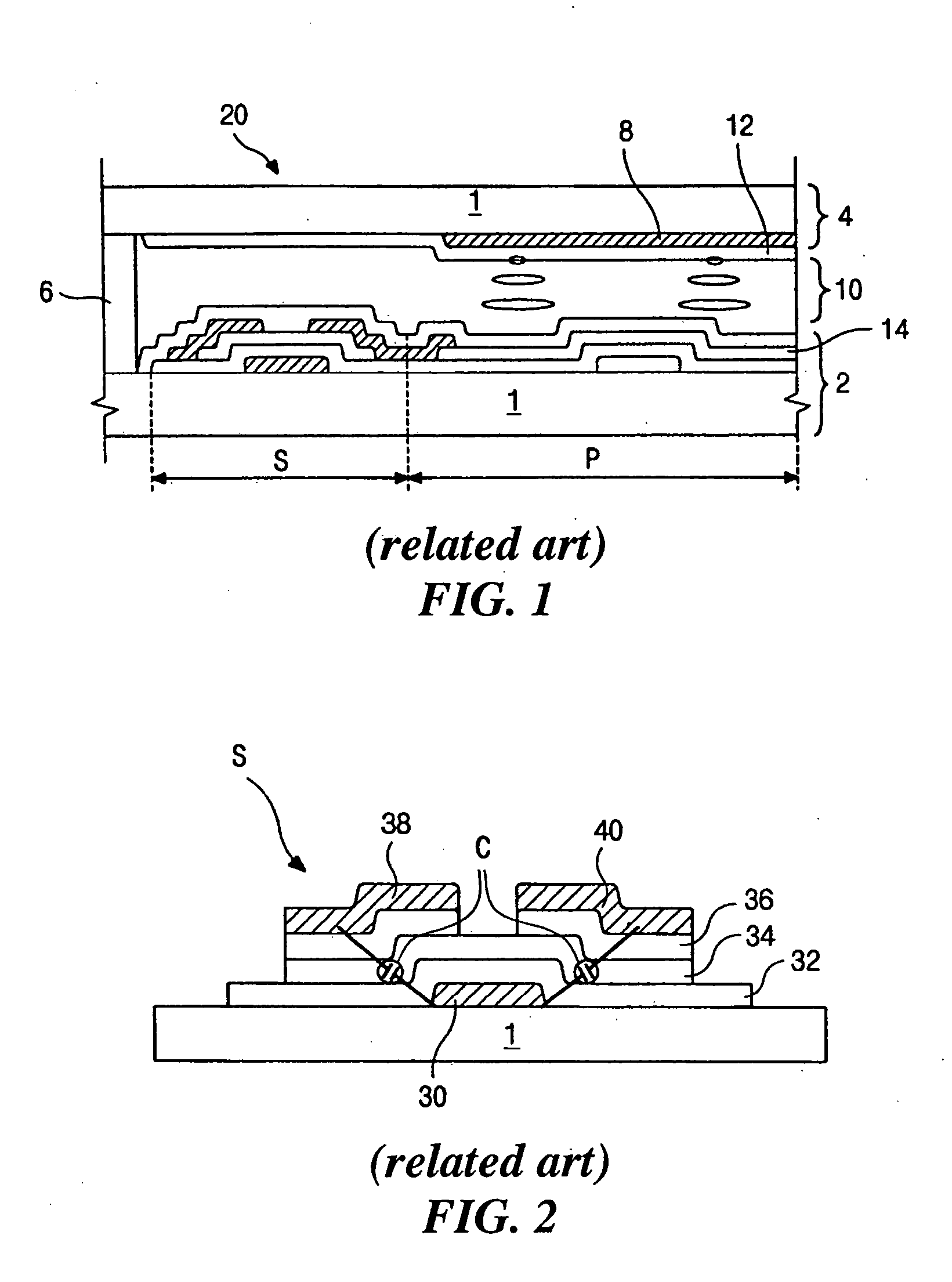
However, a thick gate electrode (gate line) may cause a break in the gate-insulating layer.
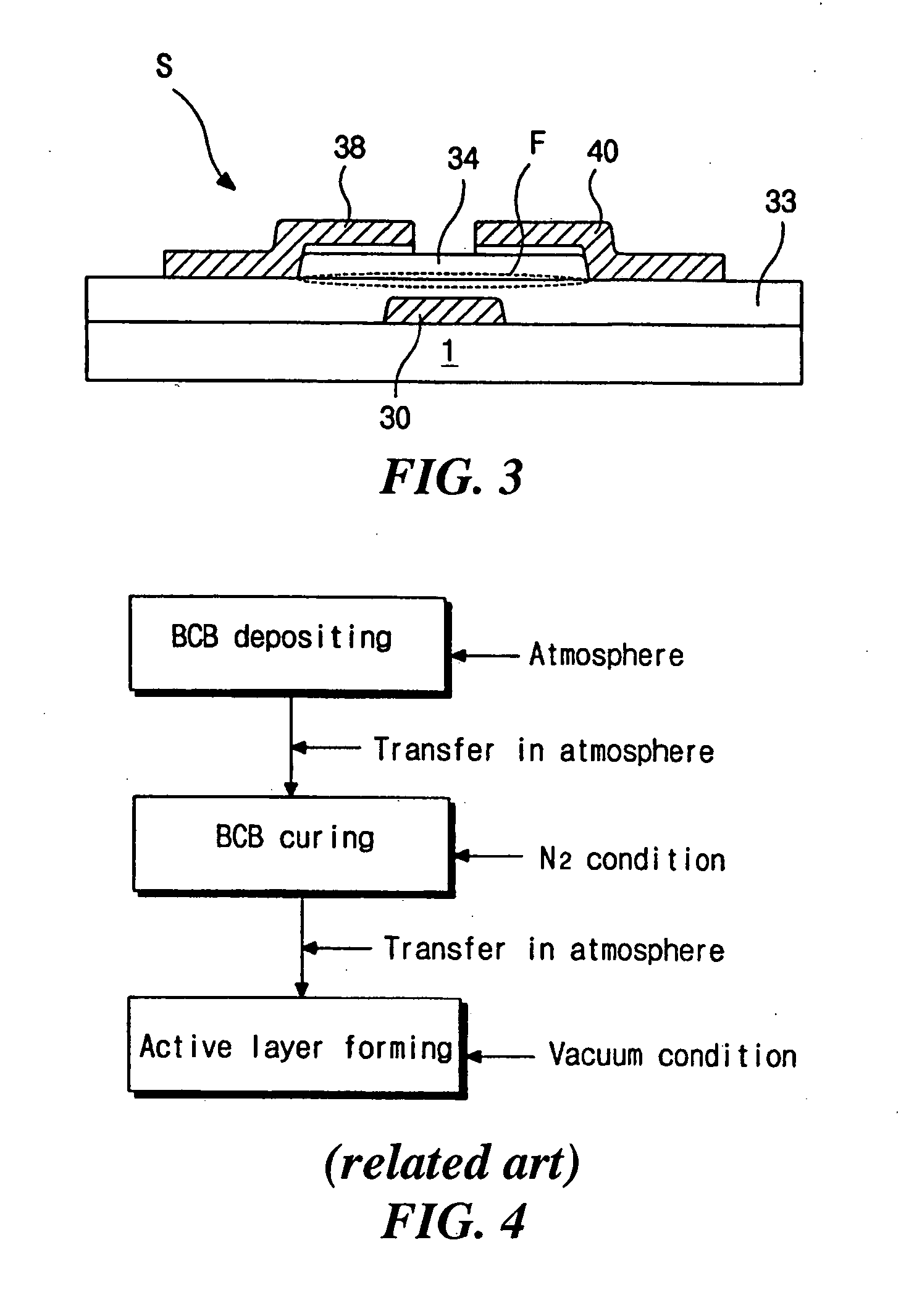
In that case, atmospheric oxygen gas may combine with the surface of the BCB film, or contaminants in the atmosphere may be attached to the surface thereof such that the BCB film is contaminated.
If the, BCB film has a contaminated surface, an interface property between the BCB gate-insulating layer and the active layer is deteriorated.
As mentioned above, if the interface “F” is poor, the electric characteristices of the TFT “S” deteriorats.
Then, the surface of the BCB film is contaminated such that the BCB gate-insulating layer made of the BCB film and the active layer which will be formed later have a poor interface property therebetween.

Method used


Image

  • Method of fabricating a thin film transistor and manufacturing equipment
  • Method of fabricating a thin film transistor and manufacturing equipment
  • Method of fabricating a thin film transistor and manufacturing equipment

Examples


Embodiment Construction

[0042] Reference will now be made in detail to the illustrated embodiments of the present invention, an example of which is shown in the accompanying drawings.

[0043]FIG. 5 illustrates a vacuum equipment 100, which is used for fabricating a BCB gate-insulating layer (reference 33 of FIG. 3) of a thin film transistor (reference “S” of FIG. 3), according to the preferred embodiment of the present invention. The inventive vacuum equipment 100 has a preparation chamber 50, which is unified with first to third reaction chambers 60, 70, and 80. The first reaction chamber 60 is used for curing the BCB gate-insulating layer, whereas the second and third reaction chambers 70 and 80 are used for forming an active layer. Each of the first to third reaction chambers 60 to 80 preferably has a heat plate (not shown) that controls a temperature of the reaction chamber. Each heat plate (not shown) of the first to third reaction chambers 60 to 80 serves to control a temperature of elements or layers...


PUM

PropertyMeasurementUnit
temperatureaaaaaaaaaa
dielectric constantaaaaaaaaaa

Abstract

A method of forming a thin film transistor includes forming a gate electrode on a substrate, forming an organic layer over the substrate having the gate electrode, curing the organic layer in a first chamber, transferring the substrate having the organic layer from the first chamber to a second chamber without exposing the substrate having the organic layer to oxygen atmosphere during transfer, forming an active layer on the organic layer in the second chamber; and forming source and drain electrodes on the active layer.

Description

[0001] This application claims the benefit of Korean Patent Application No. 2000-26788, filed on May 18, 2000, the entirety of which is hereby incorporated by reference. BACKGROUND OF THE INVENTION [0002] 1. Field of the Invention [0003] The present invention relates to a thin film transistor (TFT), and more particularly, to a TFT having an organic gate-insulating layer. [0004] 2. Discussion of the Related Art [0005] A thin film transistor (TFT) is generally used as a switching device. For example, a liquid crystal display (LCD) device widely adopts the TFT for its switching device. Since the TFT is relatively easy to form on large, relatively inexpensive, glass substrates, the TFT is one of the most focused-on devices. [0006] LCDs are based on the optical anisotropy of a liquid crystal (LC). A LC has long, thin molecules whose orientational alignment can be controlled by an applied electric field. When the alignment of the LC molecules is appropriately controlled, an applied light ...

Claims


Application Information

Patent Timeline
Patent Type & Authority Applications(United States)
IPC IPC(8): H01L21/00H01L21/336H01L29/49
CPCH01L21/67207H01L29/66765H01L29/4908H01L21/67236H01L29/786
Inventor PARK, YONG-INKIM, WOONG-KWON
Owner LG DISPLAY CO LTD
Learn More