Low noise CMOS amplifier for imaging sensors

a low-noise, amplifier technology, applied in the field of cmos imaging devices, can solve the problems of limiting scalability, increasing fixed pattern noise, increasing power dissipation, etc., and achieve the effect of increasing amplifier gain and low-noise amplification

Inactive Publication Date: 2005-03-31
INNOVATIVE TECH LICENSING
View PDF20 Cites 11 Cited by
  • Summary
  • Abstract
  • Description
  • Claims
  • Application Information

AI Technical Summary

Benefits of technology

[0011] In general, the present invention is an active pixel sensor circuit having a feedback amplifier configured as a cascoded inverter, which provides increased amplifier gain, while still providing low noise amplification.

Problems solved by technology

Active-pixel circuits also may increase power dissipation relative to passive-pixel alternatives, increase fixed pattern noise (possibly requiring additional circuitry to suppress the noise), and limit scalability.
However, this invention neither addresses scalability nor compatibility with foundry processes since floating gates transparent to all wavelengths of interest are not generally available.
Furthermore, the sampling node is vulnerable to discharge due to stray light.
U.S. Pat. No. 6,566,697, entitled PINNED PHOTODIODE FIVE TRANSISTOR PIXEL, inventors Fox et al. is compatible with production at standard CMOS processes, but is not directly scalable since it comprises five transistors.
Further, the high impedance node 18 generates reset noise and is vulnerable to pickup of feed-through offsets that create fixed pattern noise.

Method used


Image

  • Low noise CMOS amplifier for imaging sensors
  • Low noise CMOS amplifier for imaging sensors
  • Low noise CMOS amplifier for imaging sensors

Examples


Embodiment Construction

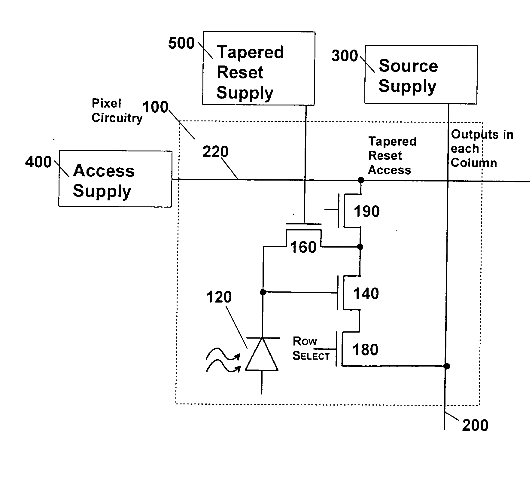
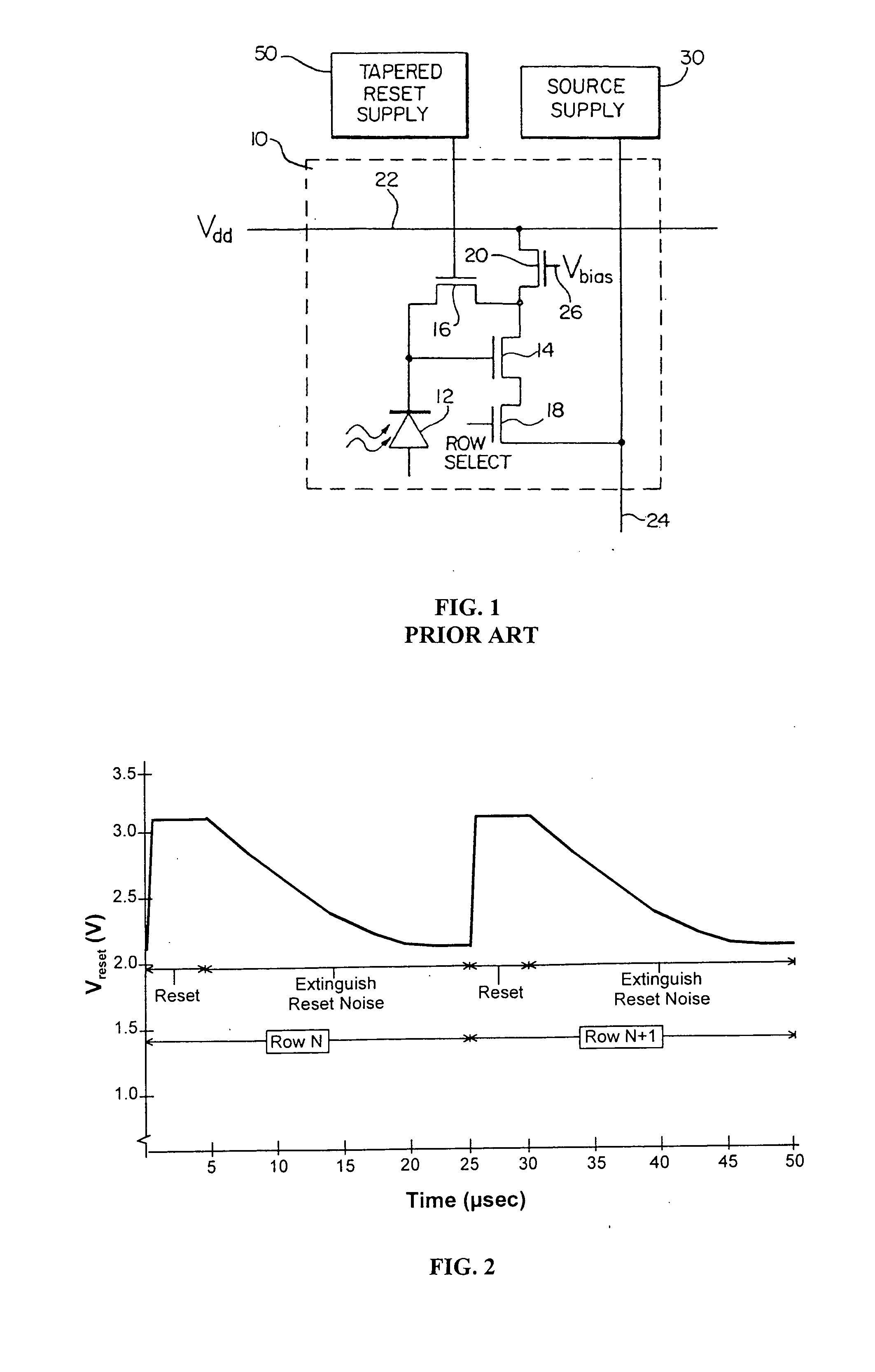
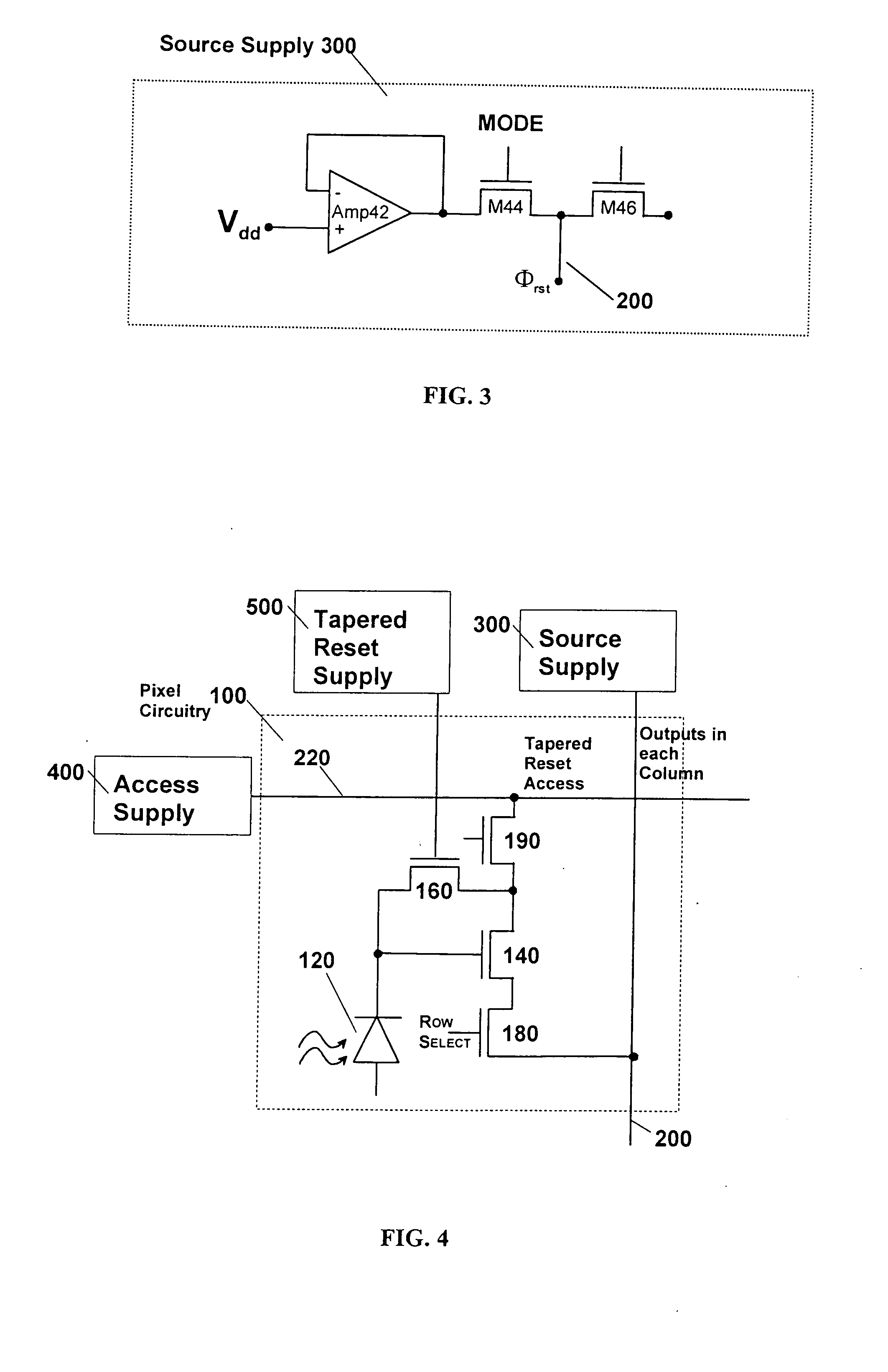
[0019] The following description is provided to enable any person skilled in the art to make and use the invention and sets forth the best modes contemplated by the inventor for carrying out the invention. Various modifications, however, will remain readily apparent to those skilled in the art, since the basic principles of the present invention have been defined herein specifically to provide a low noise amplifier for CMOS image sensors. Any and all such modifications, equivalents and alternatives are intended to fall within the spirit and scope of the present invention.

[0020] The present invention has the advantages of full process compatibility with standard salicided (self-aligned silicide) submicron CMOS. This helps maximize yield and minimize die cost because the circuit complexity is distributed amongst the active-pixels and peripheral circuits, and exploits signal-processing capability inherent to CMOS. The invention's spectral response is broad from the near-ultraviolet (4...


PUM


Abstract

A CMOS pixel amplifier circuit includes four transistors having the same polarity, and a photodetector. An access supply connects to the pixel circuit via a bus and is configured as a current source that acts as a distributed feedback amplifier, when it is connected to the pixel transistors. The access supply connects to an access MOSFET that isolates a common node from an output node. In this configuration, the feedback amplifier is a cascoded inverter, which provides gains 100-1000 times greater than prior circuits.

Description

BACKGROUND OF THE INVENTION [0001] 1. Field of the Invention [0002] The present invention relates generally to CMOS imaging devices, and more particularly to a low noise amplifier for use with high performance image sensors. [0003] 2. Description of the Related Art [0004] Visible imaging systems implemented in CMOS have the potential for significant reductions in cost and power requirements in components such as image sensors, drive electronics, and output signal conditioning electronics. A video camera, for example, can be configured as a single CMOS integrated circuit supported by only an oscillator and a battery. Such a CMOS imaging system requires lower voltages and dissipates less power than a CCD-based system. These improvements translate into smaller camera size, longer battery life, and applicability to many new products. [0005] Because of the advantages offered by CMOS visible imagers, there has been considerable effort to develop active-pixel sensor (APS) devices. Active-p...

Claims


Application Information

Patent Timeline
Patent Type & Authority Applications(United States)
IPC IPC(8): H01L27/146H04N5/363H04N5/365H04N5/3745H04N9/07
CPCH01L27/146H04N5/335H04N5/23241H04N3/1568H04N25/575H04N25/65H04N25/00
Inventor KOZLOWSKI, LESTER J.
Owner INNOVATIVE TECH LICENSING
Why Eureka
Try Eureka