Reflective microelectrical mechanical structure (MEMS) optical modulator and optical display system
- Summary
- Abstract
- Description
- Claims
- Application Information
AI Technical Summary
Benefits of technology
Problems solved by technology
Method used
Image
Examples
Embodiment Construction
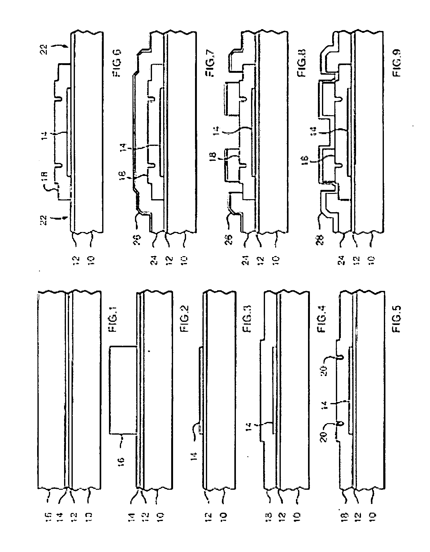
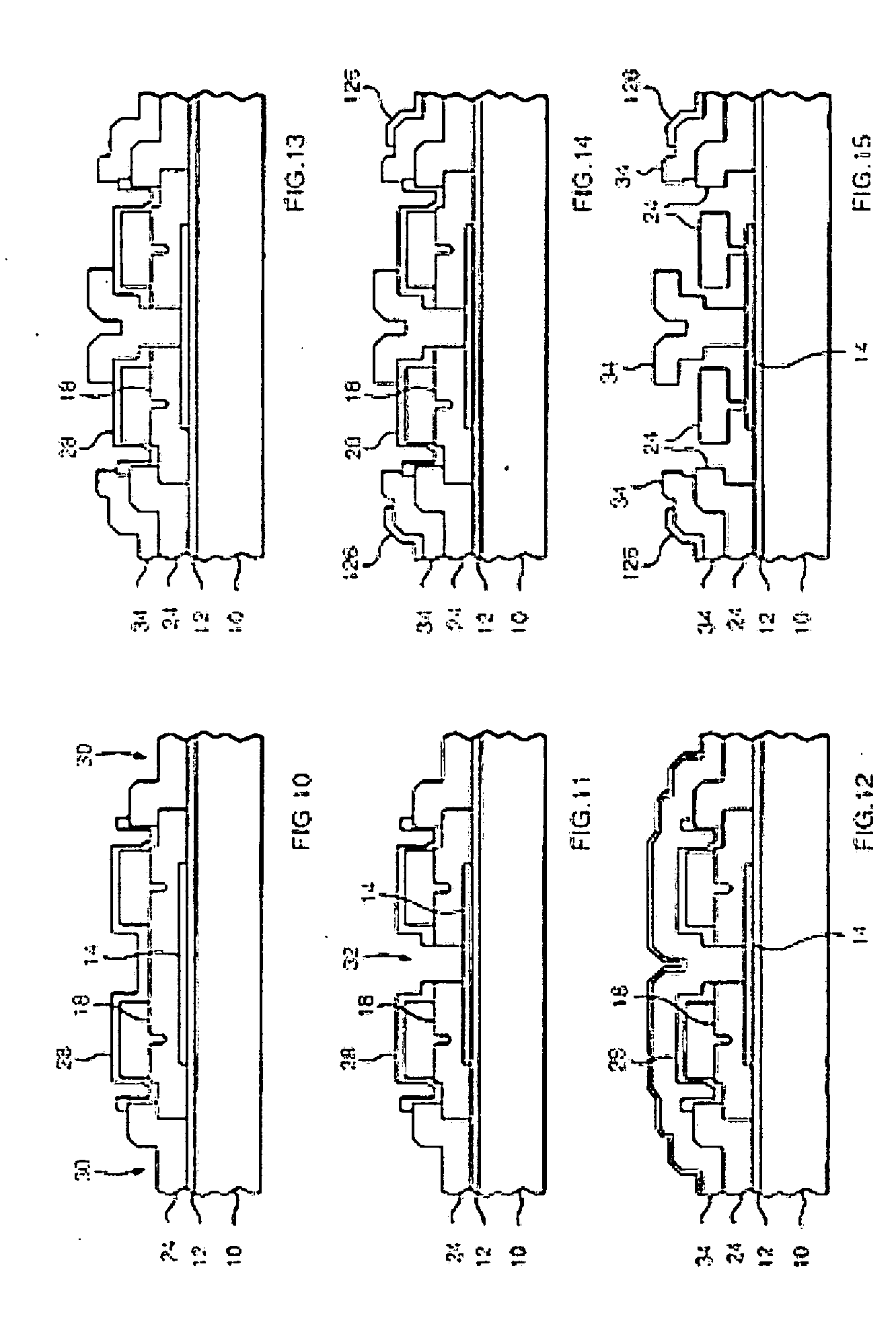
To assist with understanding the present invention, the general procedure for fabricating micromechanical devices using the MUMPs process is explained with reference to FIGS. 1-15.
The MUMPs process provides three-layers of conformal polysilicon that are etched to create a desired physical structure. The first layer, designated POLY 0, is coupled to a supporting wafer, and the second and third layers, POLY 1 and POLY 2, respectively, are mechanical layers that can be separated from underlying structure by the use of sacrificial layers that separate layers and are removed during the process.
The accompanying figures show a general process for building a micro-motor as provided by the MEMS Technology Applications Center, 3021 Cornwallis Road, Research Triangle Park, N.C.
The MUMPs process begins with a 100 mm n-type silicon wafer 10. The wafer surface is heavily doped with phosphorus in a standard diffusion furnace using POCI 3 as the dopant source. This reduces charge feed-throug...
PUM
 Abstract
Description
Claims
Application Information
 - R&D
- Intellectual Property
- Life Sciences
- Materials
- Tech Scout
- Unparalleled Data Quality
- Higher Quality Content
- 60% Fewer Hallucinations
Browse by: Latest US Patents, China's latest patents, Technical Efficacy Thesaurus, Application Domain, Technology Topic, Popular Technical Reports.
© 2025 PatSnap. All rights reserved.Legal|Privacy policy|Modern Slavery Act Transparency Statement|Sitemap|About US| Contact US: help@patsnap.com


