Room temperature ferromagnetic semiconductor grown by plasma enhanced molecular beam epitaxy and ferromagnetic semiconductor based device

a ferromagnetic semiconductor and plasma enhanced technology, applied in the direction of magnetism, crystal growth process, polycrystalline material growth, etc., can solve the problem of limitation in fabricating a spin device that can be operated at room temperatur

Inactive Publication Date: 2005-03-03
INTELLECTUAL DISCOVERY CO LTD
View PDF2 Cites 12 Cited by
  • Summary
  • Abstract
  • Description
  • Claims
  • Application Information

AI Technical Summary

Problems solved by technology

In this respect, however, (In,Mn)As (Tc=35K), (Ga,Mn)As (Tc=110K) and MnGe (Tc=116 K) are representative ferromagnetic semiconductors which have been studied up to date, but owing to the low Curie temperature, there is a limitation in fabricating a spin device that can be operated at a room temperature.

Method used


Image

  • Room temperature ferromagnetic semiconductor grown by plasma enhanced molecular beam epitaxy and ferromagnetic semiconductor based device
  • Room temperature ferromagnetic semiconductor grown by plasma enhanced molecular beam epitaxy and ferromagnetic semiconductor based device
  • Room temperature ferromagnetic semiconductor grown by plasma enhanced molecular beam epitaxy and ferromagnetic semiconductor based device

Examples


Embodiment Construction

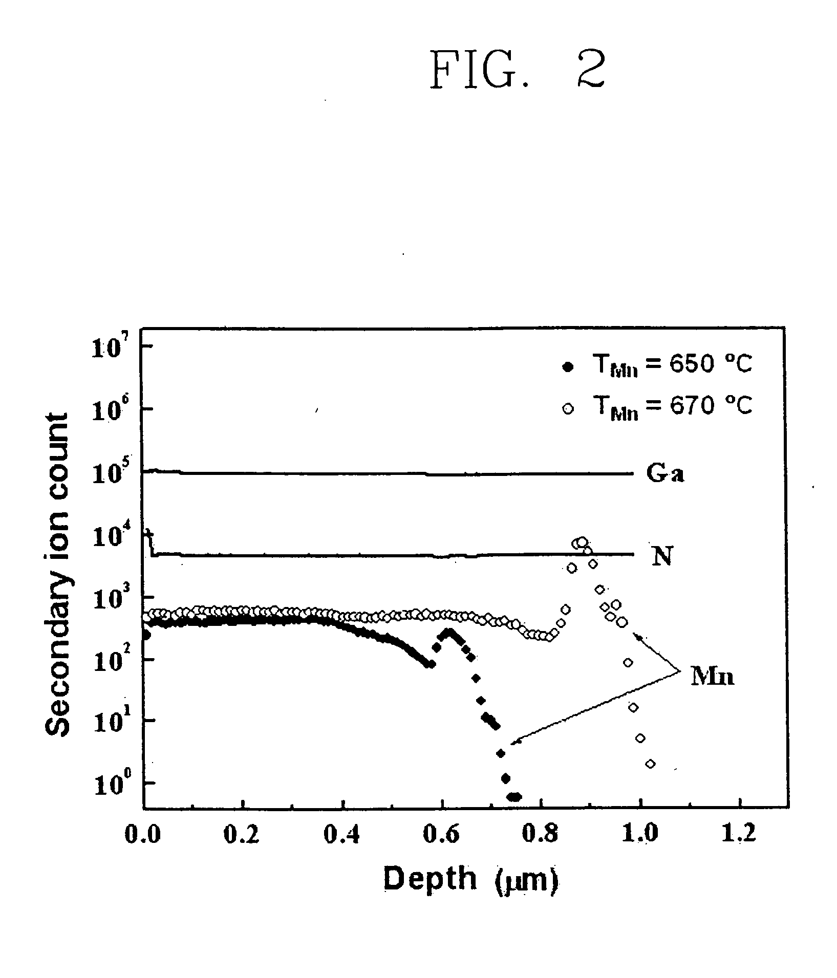
[0028] As one embodiment of the present invention, a Mn- or Mg-doped GaN thin film was grown by using a plasma-enhanced molecular beam epitaxy device, for which an undoped GaN (GaN templete) grown on a surface of sapphire (0001) by using a metal organic chemical vapor deposition (MOCVD) device was used as a substrate.

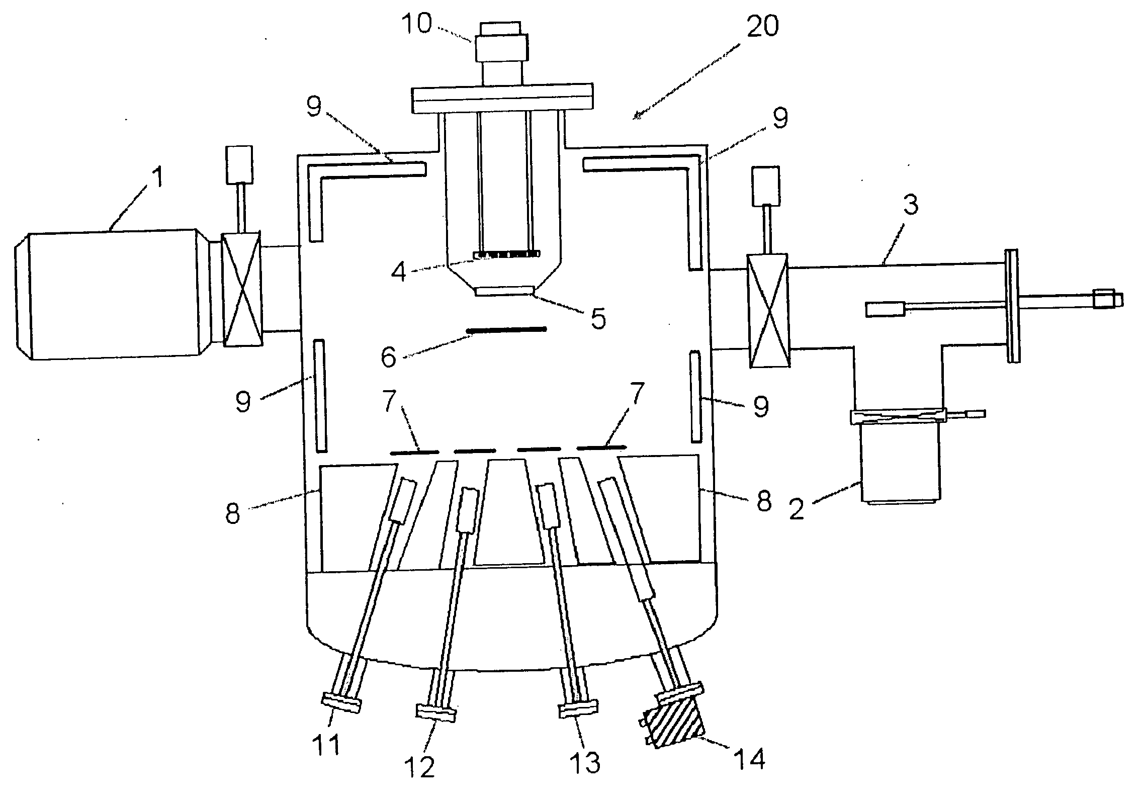
[0029]FIG. 1 is a schematic view showing the plasma-enhanced molecular beam epitaxy device used in the present invention.

[0030] Turbomolecular pumps 1 and 2 are connected at the right side and left side of a chamber 20, and a substrate 5 is positioned at an upper portion of the chamber 20. The substrate is controlled in its position by a substrate manipulator 10 formed at an upper portion of the chamber. A heater 4 is positioned at an upper side of the substrate to control a temperature of the substrate. A liquefied nitrogen (LN2) supply unit 8 is positioned at a lower portion inside the chamber and LN2 covers 9 are attached inside the chamber. Reference numerals 6 an...


PUM

PropertyMeasurementUnit
plasma poweraaaaaaaaaa
temperatureaaaaaaaaaa
temperaturesaaaaaaaaaa

Abstract

A 3 group-5 group compound ferromagnetic semiconductor, comprising one material ‘A’ selected from the group of Ga, Al and In and one material ‘B’ selected from the group consisting of N and P, wherein one material ‘C’ selected from the group consisting of Mn, Mg, Co, Fe, Ni, Cr and V is doped as a material for substituting the material ‘A’, the compound semiconductor has a single phase as a whole. The ferromagnetic semiconductor can be fabricated by a plasma-enhance molecular beam epitaxy growing method and since it shows the ferromagnetic characteristics at a room temperature, it can be applied as various spin electron devices.

Description

BACKGROUND OF THE INVENTION [0001] 1. Field of the Invention [0002] The present invention relates to a room temperature ferromagnetic semiconductor used for a spin electronic device having wide bandgap semiconductor characteristics and magnetic characteristics at a room temperature, its fabrication method, and a ferromagnetic semiconductor based device. [0003] 2. Description of the Background Art [0004] A research on a GaN-based nitride semiconductor was started to fabricate a blue light emitting device in the early 1990, and currently, researches are being actively conducted on various electronic devices in addition to light emitting and light receiving devices. [0005] In forming a triple element compound, an energy gap can be controlled from 1.9 eV to 6.2 eV, so that the nitride semiconductor is used for fabrication of a light emitting device of a wave length region of the entire visible light including an ultraviolet ray region. A blue and green light emitting diode (LED) and a u...

Claims


Application Information

Patent Timeline
Patent Type & Authority Applications(United States)
IPC IPC(8): C30B29/38H01L43/00H01F1/40H01F10/193H01F10/32H01F41/30H01L21/203H01L29/66H01L33/40H01L43/08H01L43/12
CPCB82Y25/00H01L43/10H01F1/404H01F10/193H01F10/3213H01F41/30H01L29/66984H01L33/40H01L21/02573H01L21/0242H01L21/0254H01L21/02543H01L21/02581H01L21/0262H01L21/02631H01L43/08B82Y40/00H10N50/85H10N50/10C30B29/38H10N50/00
Inventor LEE, WOO YOUNGHAN, SUK HEECHANG, JOON YEONKIM, HI JUNGLEE, JUNG MIMYOUNG, JAE MIN
Owner INTELLECTUAL DISCOVERY CO LTD
Why Eureka
Try Eureka