Method of manufacturing semiconductor device

a manufacturing method and semiconductor technology, applied in semiconductor devices, semiconductor/solid-state device details, electrical devices, etc., can solve problems such as voids that are apt to occur in encapsulating resins

Active Publication Date: 2005-02-03
LAPIS SEMICON CO LTD
View PDF2 Cites 12 Cited by
  • Summary
  • Abstract
  • Description
  • Claims
  • Application Information

AI Technical Summary

Benefits of technology

[0014] Therefore, the present invention has been made to solve the foregoing problems. An object of the present invention is to provide a resin encapsulating process capable of preventing voids from occurring in an encapsulating resin.
[0023] pressure-reducing the interior of the cavity and reducing the capacity of the cavity to cause the molten resin obtained by melting the resin to contact the first main surface, thereby forming an encapsulating portion on the first main surface.

Problems solved by technology

As a result, there was a fear that voids were apt to occur in the encapsulating resin.

Method used


Image

  • Method of manufacturing semiconductor device
  • Method of manufacturing semiconductor device
  • Method of manufacturing semiconductor device

Examples


first embodiment

[0089] An encapsulating process of a first embodiment will be explained with reference to FIGS. 6 and 7.

[0090] FIGS. 6(A) and 6(B) are respectively typical cross-sectional views for describing the encapsulating process of the first embodiment. A cut away portion or region of a cross section similar to FIG. 1(B) is typically shown.

[0091] FIGS. 7(A) and 7(B) are respectively cross-sectional views following FIG. 6, for describing the encapsulating process of the first embodiment.

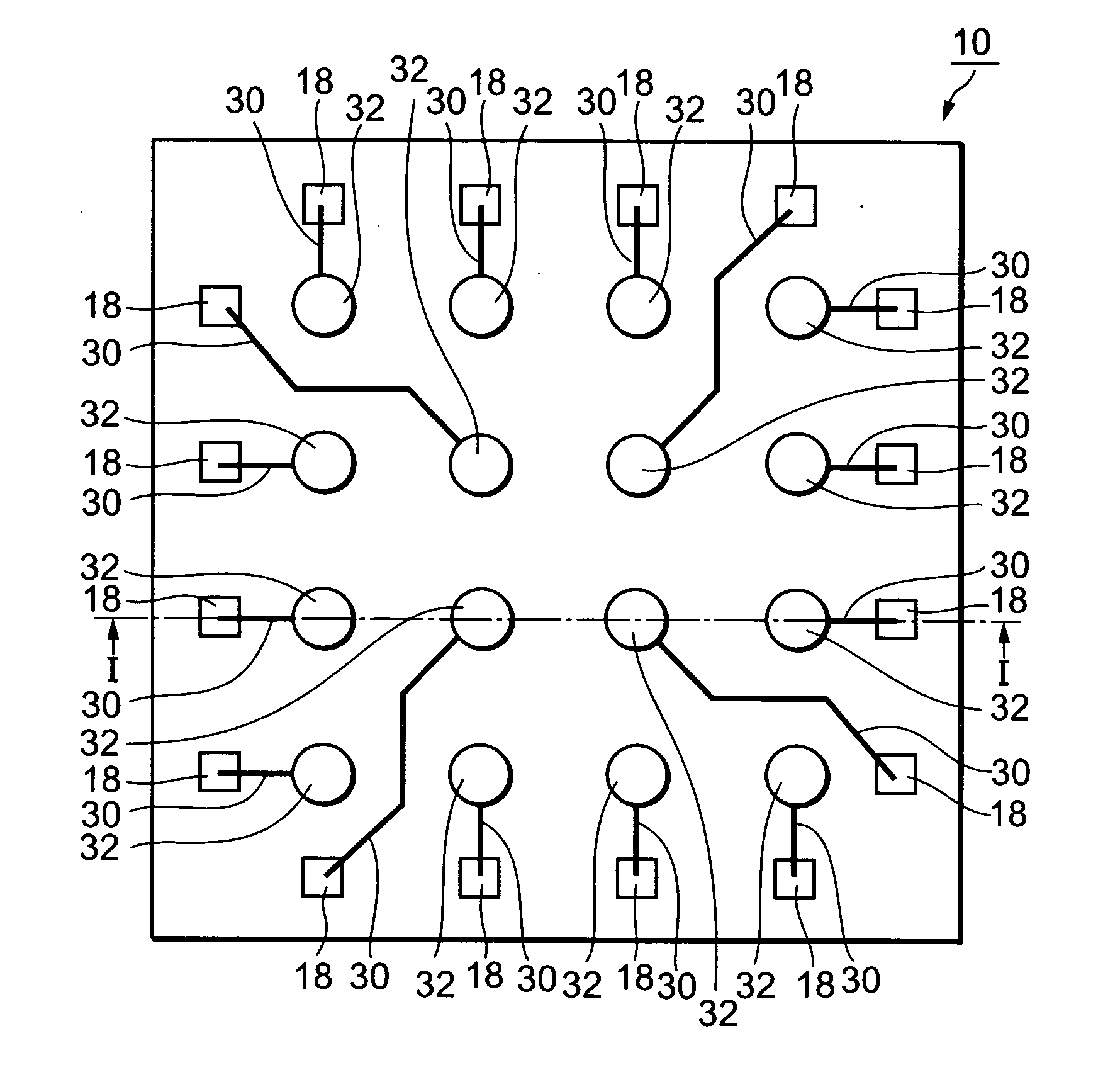
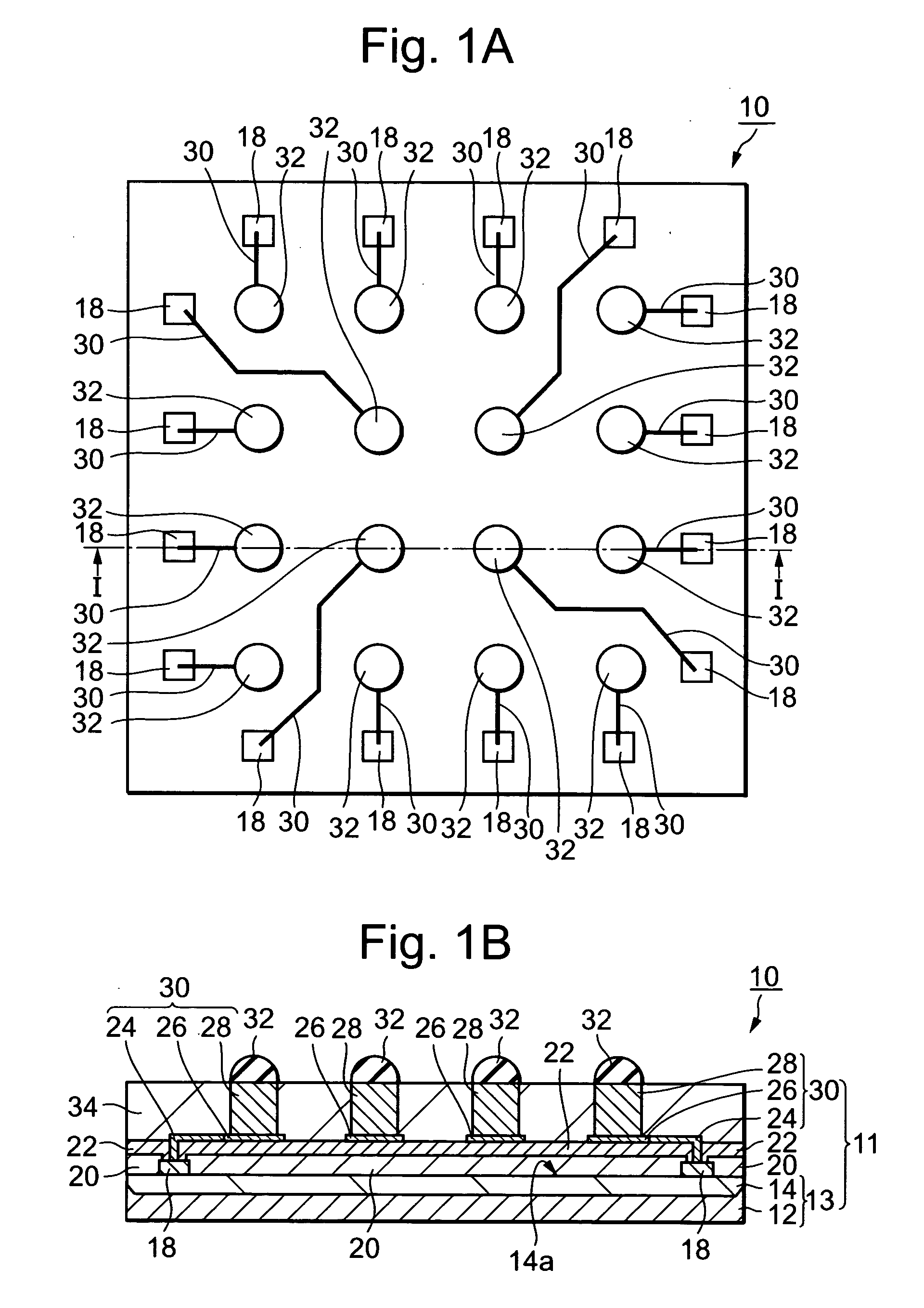
[0092] Incidentally, in the description of the following manufacturing process, a semiconductor wafer 11 will be defined as a structural body in which processing has been completed up to the process of forming the electrode posts 28 according to the wafer process shown in FIG. 3(B). In order to simplify illustrations and explanations, the device region 14, circuit element connecting pads 18, passivation film 20, insulating film 22, redistribution wiring layers 24 and electrode post pads 26, which have been a...

second embodiment

[0119] An encapsulating process of a second embodiment will be explained with reference to FIG. 8. Incidentally, since a sealing or encapsulating device 300 applied to the second embodiment is identical to the device described in the first embodiment, the detailed description of components thereof is omitted. Since a point of difference between the encapsulating process of the second embodiment and the encapsulating process of the first embodiment resides only in the formation of a resin material placed on a stage 220, the detailed description of the same process steps is omitted.

[0120] FIGS. 8(A) and 8(B) are typical cross-sectional views for describing the encapsulating process of the second embodiment. A cut away portion or region of a section similar to FIG. 1(B) is typically illustrated.

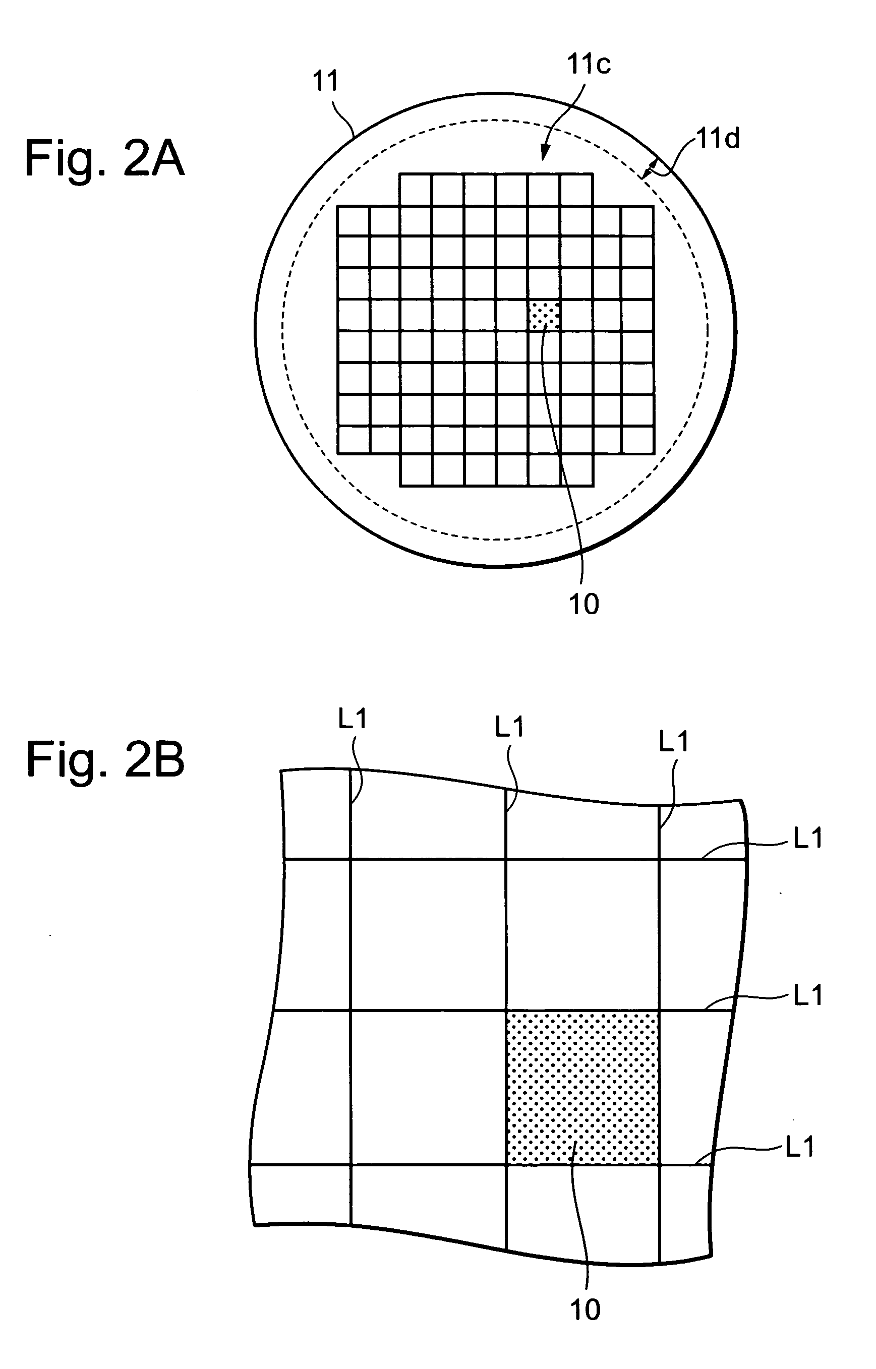
[0121] As shown in FIG. 8(A), a semiconductor wafer 11 is placed on a substrate support region 110a of a clamp 110 in such a manner that the peripheral region 11d of the semiconductor wafer 11...


PUM


Abstract

A method of manufacturing a semiconductor device includes preparing a semiconductor wafer including a first main surface having a semiconductor device forming region and a peripheral region, and a second main surface; preparing first and second dies defining a cavity; holding the semiconductor wafer by the first die so that the first main surface is exposed; placing a film member on the second die; supplying a predetermined amount of resin to a predetermined region on a resin layout region of the film member; heating the first die and the second die; bringing the first die and the second die into contact with each other through the film member to form the cavity, thereby the first main surface and the resin are placed in the cavity; and pressure-reducing the interior of the cavity and reducing the capacity of the cavity to cause the molten resin obtained by melting the resin to contact the first main surface, thereby forming an encapsulating portion on the first main surface.

Description

BACKGROUND OF THE INVENTION [0001] 1. Field of the Invention [0002] The present invention relates to a method of manufacturing a semiconductor device, and particularly to a method of manufacturing a semiconductor device, which is effective for application to a WCSP (Wafer Level Chip Size Package) in which a packaging process step is executed in a wafer process. [0003] This application is counterpart of Japanese patent applications, Serial Number 284526 / 2003, filed Jul. 31, 2003, and Serial Number 89168 / 2004, filed Mar. 25, 2004, the subject matter of which is incorporated herein by reference. [0004] 2. Description of the Related Art [0005] A package having a size substantially equivalent to that of a semiconductor chip is generally called “CSP (Chip Size Package)”. CSPs obtained by packaging semiconductor chips formed in a semiconductor wafer while a semiconductor wafer state is being held as it is and bringing it into fractionalization, are called “WCSPs”. [0006] As a resin encapsu...

Claims


Application Information

Patent Timeline
IPC IPC(8): H01L23/12H01L21/44H01L21/56H01L23/31
CPCH01L21/565H01L21/566H01L23/3114H01L2924/0002H01L2924/00
Inventor EGAWA, YOSHIMISUGAI, AKIRA
Owner LAPIS SEMICON CO LTD
Why Eureka
Try Eureka