Process to improve image sensor sensitivity

a technology of image sensor and process, applied in the field of image sensor and packaging methods thereof, can solve the problems of inability to achieve the desired optical properties of image sensors, inability to achieve the desired optical properties, etc., to achieve the effect of improving the sensitivity of the sensor

Inactive Publication Date: 2005-01-06
TAIWAN SEMICON MFG CO LTD
View PDF5 Cites 8 Cited by
  • Summary
  • Abstract
  • Description
  • Claims
  • Application Information

AI Technical Summary

Benefits of technology

Accordingly, it is the object of this invention to provide a packaged image sensor with improved image sensitivity.

Problems solved by technology

The beneficial electrical and mechanical attributes of packaging can, however, adversely impact the required optical properties of the image sensors.
Although the bonding agent is kept to a minimum thickness consistent with requirements of structural integrity, it causes an inevitable degradation of the optical signal impinging on and propagating within the optically sensitive region.
Although the radius of curvature of the microlens can be adjusted to shorten the focal length, this method has process and physical limits.

Method used


Image

  • Process to improve image sensor sensitivity
  • Process to improve image sensor sensitivity
  • Process to improve image sensor sensitivity

Examples


first embodiment

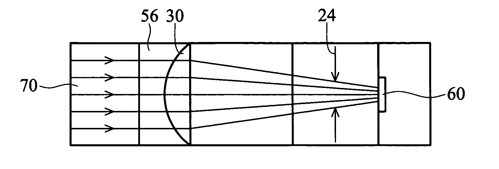
Referring next to FIG. 4, the packaging method of the present invention is shown, wherein an additional intermediate optically refractive layer (56) with nI<nB is formed between the microlens (30) and the bonding layer (70). For example, while the bonding layer of epoxy has nB=1.5, the additional intermediate optically refractive layer (56) has nI<1.5, where nI between approximately 1.33 and 1.45 is preferred. This additional intermediate optically refractive layer (56) has the characteristics of high transmittance (>90%, greater than 95% is preferred), thermal resistance, chemical resistance and viscosity greater than 5 mpas (greater than 10 mpas is preferred), and can be a layer of material such as [A] a mixture including Fluororesin derivative, Initatoe, Methylisobutylketone (MIBK), and t-butanol, or [B] a mixture including Fluororesin derivative, Initatoe, Melamine resin, Methylisobutylketone (MIBK), t-butanol, formed to a thickness higher than microlens (30), approxim...

third embodiment

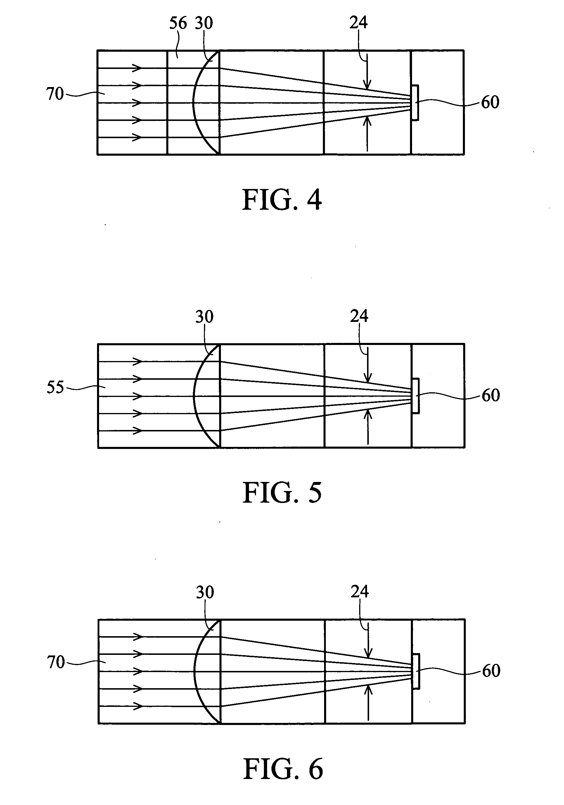
Referring finally to FIG. 6, there is shown in cross-sectional schematic form, the present invention wherein the microlens (30) is now formed of a transparent material having an index of refraction nL satisfying nL−nB greater than 0.2. For example, the epoxy layer (70) has an index of refraction nB approximately 1.5, and the index of refraction nL of the microlenses (30) is greater than 1.7, with a range between 1.73 and 1.8 being preferred.


PUM


Abstract

A packaged image sensing device of improved sensitivity is formed by providing a mechanism for enhancing the focusing of embedded microlenses on the photosensitive elements of the image sensor. Normally, the bonding material interposed between the packaging layers and the microlenses defocuses the microlenses. In one embodiment of the present invention, the focus is restored by interposing an intermediate optically refractive layer between the bonding material and the lenses. In another embodiment, a bonding material with a lower index of refraction is used. In a final embodiment, the microlenses are formed in a material of a higher index of refraction.

Description

BACKGROUND OF THE INVENTION 1. Field of the Invention This invention relates generally to image sensors and packaging methods thereof. In particular, it relates to the formation of either a CMOS (CIS) or charge-coupled device (CCD) packaged image sensor having embedded microlenses and improved sensitivity as a result of a novel packaging process. 2. Description of the Related Art Solid state image sensors are necessary components in many optoelectronic devices, including digital cameras, cellular phones, and toys. In the simplest possible terms, such a sensor consists of an array of photosensors (eg. photodiodes), connected to solid state devices that convert the signals generated by the photosensors (typically electrical charge) into forms that can be displayed electronically. Two types of signal converting solid state devices in common use are charge-coupled devices (CCDs) and CMOS image sensors (CISs). In order for these devices to operate at optimal levels, the light from th...

Claims


Application Information

Patent Timeline
IPC IPC(8): G02B3/00G02B27/09H01L27/146H01L27/148H04N5/335
CPCG02B3/0012G02B27/09G02B3/0056
Inventor HSU, HUNG-JENCHANG, CHIU-KUNGWONG, FU-TIENTSENG, TE-FU
Owner TAIWAN SEMICON MFG CO LTD
Why Eureka
Try Eureka