Biochemical ultrasensitive charge sensing
- Summary
- Abstract
- Description
- Claims
- Application Information
AI Technical Summary
Benefits of technology
Problems solved by technology
Method used
Image

Examples
Embodiment Construction
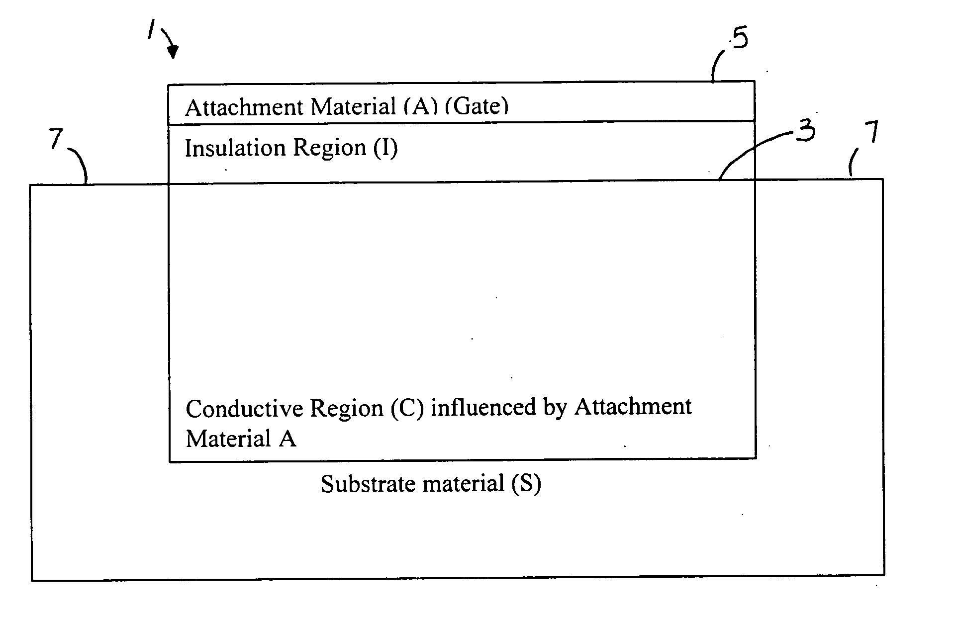
[0058]FIGS. 1 and 2 show the general principle of the present invention. FIG. 1 is a schematic representation of a charge sensing device 1. A substrate material S has an insulation region I coated on a surface portion 3. An attachment material A, which forms a gate 5 is coated on the insulation region. The attachment material A influences conductive region C. Contacts 7 are provided on the substrate S at opposite portions. A conducting region is located beneath a gate-influencing region where the charge on the gate affects a conducting C region of the charge sensing device.
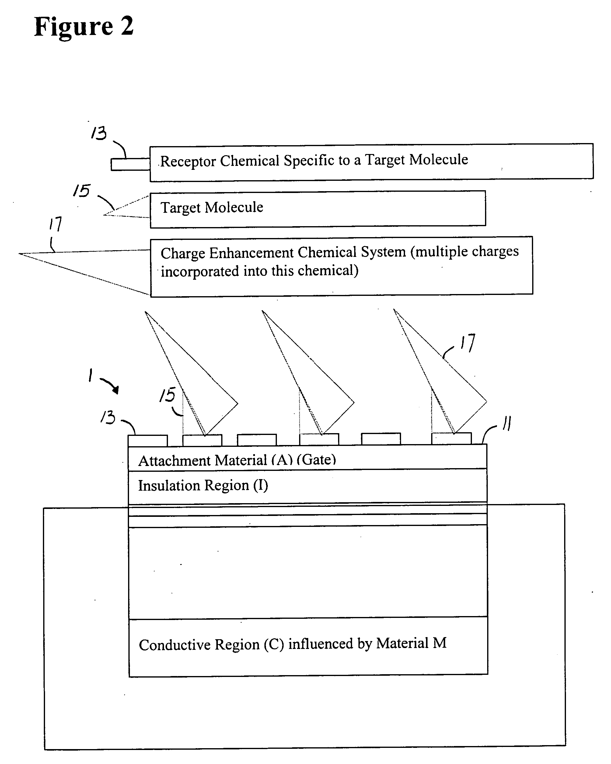
[0059]FIG. 2 shows a generic semiconductor charge ultrasensitive sensing device 1. In this figure, only a portion of the sensor affected by a gate charge or potential change changes the underlying conductive region C. The device of FIG. 1 is coated with a material 11 to which chemicals 13 are attached, which are in turn specific binders to other molecules 15, such as an antibody binding to an antigen, or an oligo...
PUM
 Abstract
Description
Claims
Application Information
 - R&D
- Intellectual Property
- Life Sciences
- Materials
- Tech Scout
- Unparalleled Data Quality
- Higher Quality Content
- 60% Fewer Hallucinations
Browse by: Latest US Patents, China's latest patents, Technical Efficacy Thesaurus, Application Domain, Technology Topic, Popular Technical Reports.
© 2025 PatSnap. All rights reserved.Legal|Privacy policy|Modern Slavery Act Transparency Statement|Sitemap|About US| Contact US: help@patsnap.com