
Method for manipulating data in a group of processing elements

a data and processing element technology, applied in the field of parallel processing, can solve the problems of special machines, excluded from mass market applications, and high cost of active memory computers

Active Publication Date: 2004-10-28
MICRON TECH INC
View PDF41 Cites 17 Cited by
  • Summary
  • Abstract
  • Description
  • Claims
  • Application Information

AI Technical Summary

Benefits of technology

The present invention relates to methods for manipulating data in a parallel processing system, specifically in an active memory device or single instruction, multiple data (SIMD) computer. The invention provides methods for performing a reflection of data, transposing data, and rotating data in a matrix of processing elements. These methods enable data to be processed close to where it is stored, reducing the workload on the central processing unit (CPU) and improving performance. The invention also includes an efficient mechanism for moving data from one processing element to another, enabling independent processing of data within the array. Overall, the invention provides a way to effectively use the vast data bandwidth and processing power available in active memory devices or SIMD computers.

Problems solved by technology

However, until the advent of integrated logic and current DRAM technologies, active memory computers were always expensive, special machines, excluded from mass market applications.

Method used


Image

  • Method for manipulating data in a group of processing elements
  • Method for manipulating data in a group of processing elements
  • Method for manipulating data in a group of processing elements

Examples


Embodiment Construction

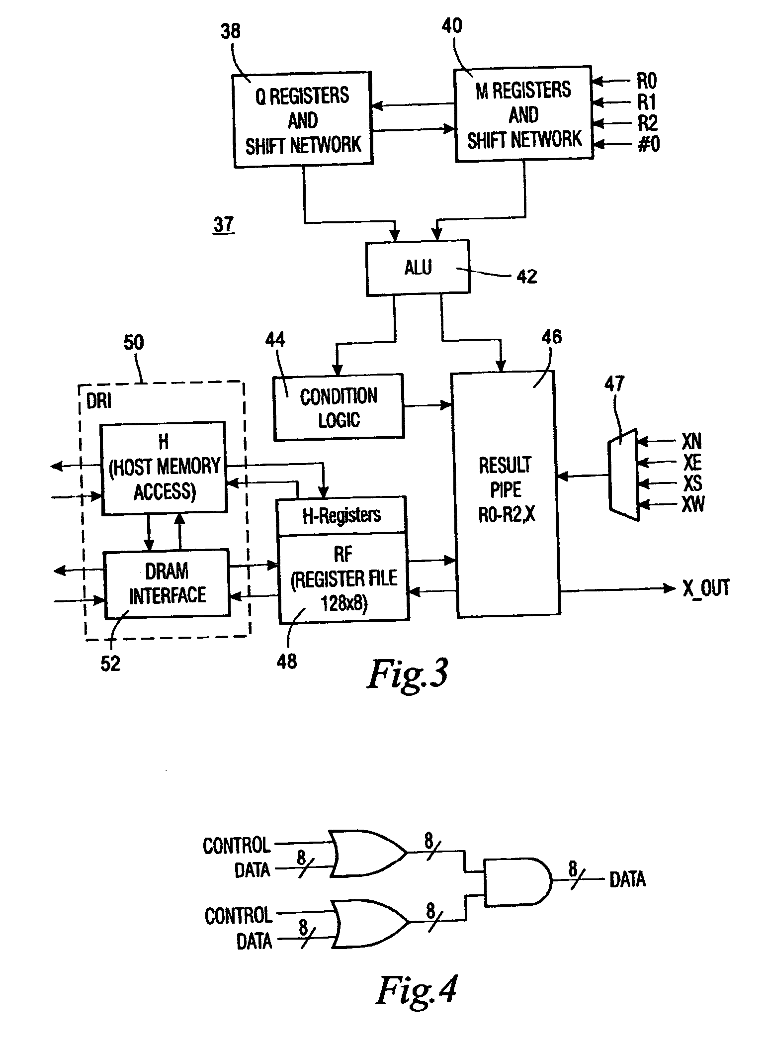
[0030] Illustrated in FIG. 2 is a high level block diagram of one example of an active memory device 18 on which the methods of the present invention may be practiced. The reader should understand that the methods of the present invention are generally applicable to any group of processing elements having the necessary physical connections between PEs to enable the manipulation of data as required by the methods. The hardware illustrated in FIG. 2 is disclosed for purposes of illustration and not limitation. Furthermore, those of ordinary skill in the art will recognize that the block diagram of FIG. 2 is an overview of an active memory device with a number of components known in the art being omitted for purposes of clarity.

[0031] The active memory device 18 of FIG. 2 is intended to be deployed in a computer system as a slave device, where a host processor (e.g. CPU 12 in FIG. 1) sends commands to the active memory device 18 to initiate processing within the active memory device 18...


PUM


Abstract

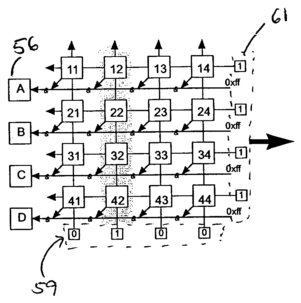
The present invention is capable of placing or loading input data into a 2D or 3D array of processing elements interconnected in a variety of ways, and moving the data around by using a combination of shifts, e.g. north, south, east, west, which can be combined in any desired manner. The exact type and combination of shifts depends upon the particular data manipulation desired. As the shifting proceeds, each processing element is presented with a plurality of different array values. Each processing element can conditionally load any of the values it sees into the output result. The timing of the loading is achieved by monitoring a local counter. In a preferred embodiment, when the value in the local counter is non-positive, the current array value is selected as the final output for the output result. In general, each local counter is initialized to a different positive value and, at certain points in the shifting process, the counter is decremented. The initial value of the counter depends upon its location, and is given by the general function f(x_Index, y_Index, z_Index), with the exact form of f( ) depending upon the particular data manipulation desired.

Description

[0001] The present application is related to the following applications: Method for Manipulating Data in a Group of Processing Elements to Perform a Reflection of the Data (docket no. DB001071-000); Method for Manipulating Data in a Group of Processing Elements to Transpose the Data (docket no. DB001070-000); Method for Manipulating the Data in a Group of Processing Elements to Transpose the Data Using a Memory Stack (docket no. DB001069-000); and Method of Rotating Data in a Plurality of Processing Elements (docket no. DB001063-000), all filed concurrently herewith.BACKGROUND OF INVENTION[0002] The present invention relates generally to parallel processing and, more specifically, to parallel processing in an active memory device or single instruction, multiple data (SIMD) computer.[0003] A single, synchronous dynamic random access memory (SDRAM) chip has an internal data bandwidth of greater than 200 G bits / s and a very wide data bus (thousands of bits). That vast data bandwidth pr...

Claims


Application Information

Patent Timeline
Patent Type & Authority Applications(United States)
IPC IPC(8): G06F9/312G06F9/38G06F15/00G06F15/78
CPCG06F9/30036G06F9/30043G06F15/7821G06F9/3879G06F9/3887G06F9/3877
Inventor BEAUMONT, MARK
Owner MICRON TECH INC
Learn More