
Changing scan cell output signal states with a clock signal

a clock signal and scan cell technology, applied in the field of integrated circuits, can solve the problems of increasing the complexity of the board level testability, the difficulty of in-circuit testing of the board, and the difficulty of the traditional method of probing the board, so as to facilitate boundary test and reduce the overall test time

Inactive Publication Date: 2004-10-07
WHETSEL LEE D JR
View PDF99 Cites 18 Cited by
  • Summary
  • Abstract
  • Description
  • Claims
  • Application Information

AI Technical Summary

Benefits of technology

[0007] In accordance with the present invention, a boundary scan test system is provided which substantially eliminates the disadvantages and problems associated with prior testing systems.
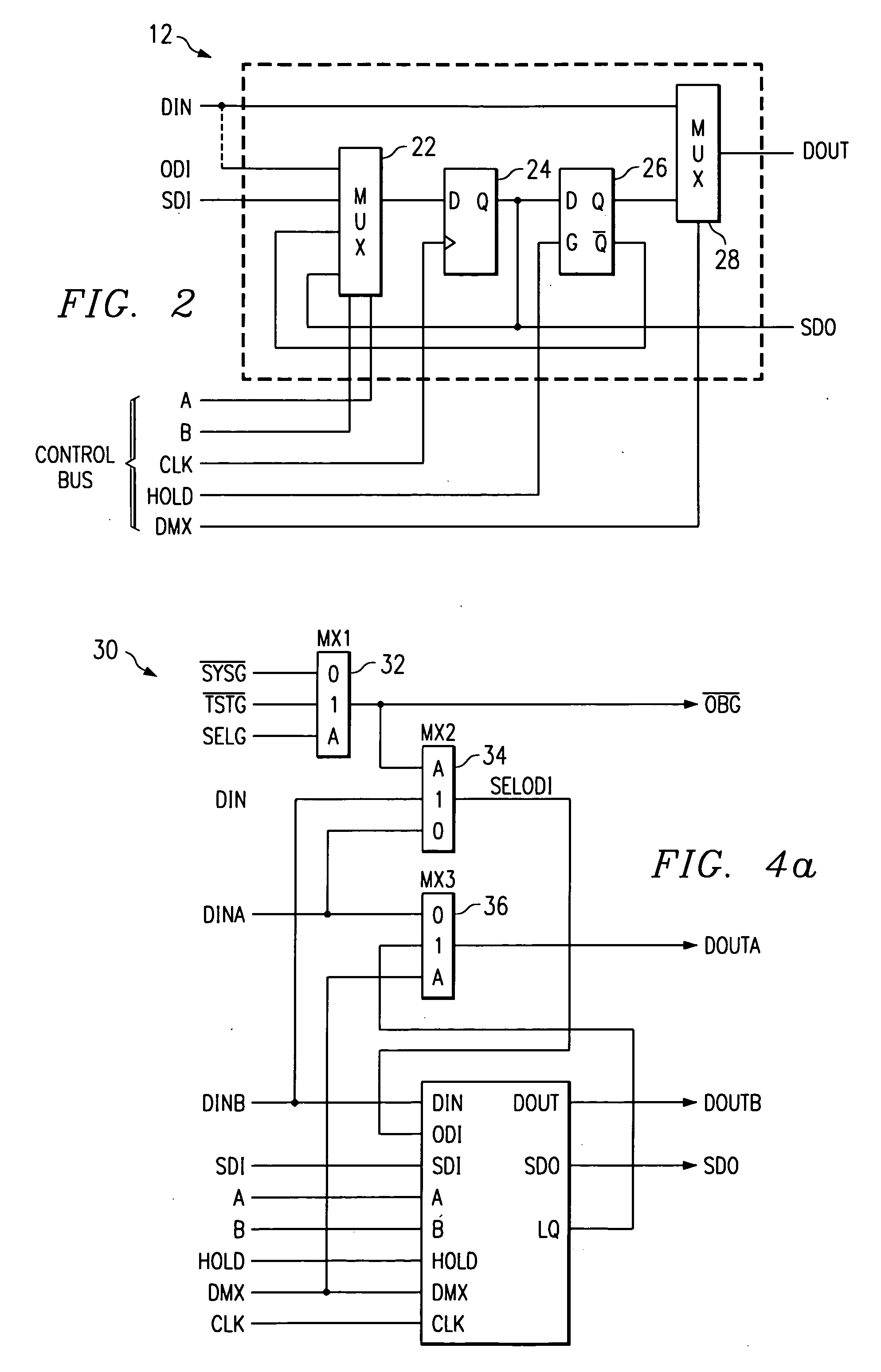
[0009] The present invention provides a variety of functions for testing purposes. The test cell is operable to both reserve data inputs and control data outputs to and from the cell. The test cell may operate in two modes: "normal" mode and "testing" mode. In normal mode, the test cell provides a data path through which inputs and outputs may propagate freely through the test cell. While in the normal mode, the test cell can also load and shift test data, remain in an idle state, or toggle test data without disturbing the normal operation of the integrated circuit. Further, while in normal mode, a predetermined test data bit may be inserted into the data stream. Also, the test cell may perform a self-test while in the normal mode to insure correct operation of the test cell.
[0011] The present invention provides significant advantages over the prior art. First, the test cell of the present invention may be used to perform internal and external boundary testing simultaneously, in order to reduce overall test time. Second, the test cells are capable of sampling or inserting data at the boundary during normal operation of the host integrated circuit. Third, the test cell is synchronous in operation with a free running test clock. Fourth, the present invention provides a method of toggling an IC's output buffers, independent of the IC's application logic, in order to achieve parametric measures and to facilitate boundary test. Fifth, the test cell provides self-testing capabilities.

Problems solved by technology

Due to advances in the fields of board interconnect technology, surface mount packaging and IC density, board level testability is becoming increasingly complex.
The combination of advanced board interconnect technology, such as buried wire interconnects and double-sided boards, along with surface mount packaging creates problems for in-circuit testing of the boards.
As board density (the number of ICs on a board) increases, the process of probing the board using traditional techniques becomes more difficult, due to the lack of physical access.
When such test is being applied to one IC on a board, neighboring ICs, whose output buffers are tied to the same nodes, may be damaged.

Method used


Image

  • Changing scan cell output signal states with a clock signal
  • Changing scan cell output signal states with a clock signal
  • Changing scan cell output signal states with a clock signal

Examples


Embodiment Construction

[0029] The preferred embodiment of the present invention is best understood by referring to FIGS. 1-5 of the drawings, like numerals being used for like and corresponding parts of the various drawings.

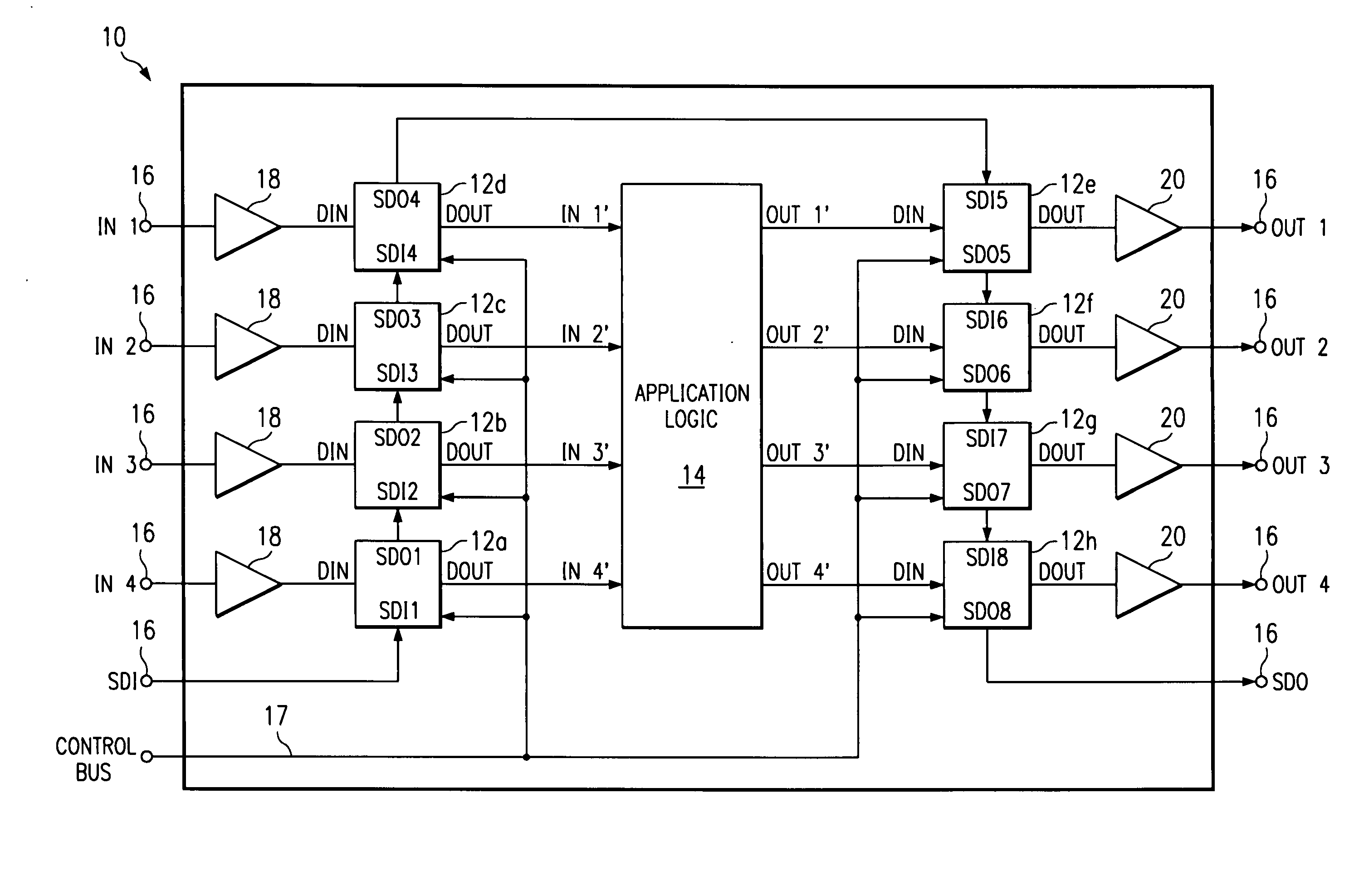
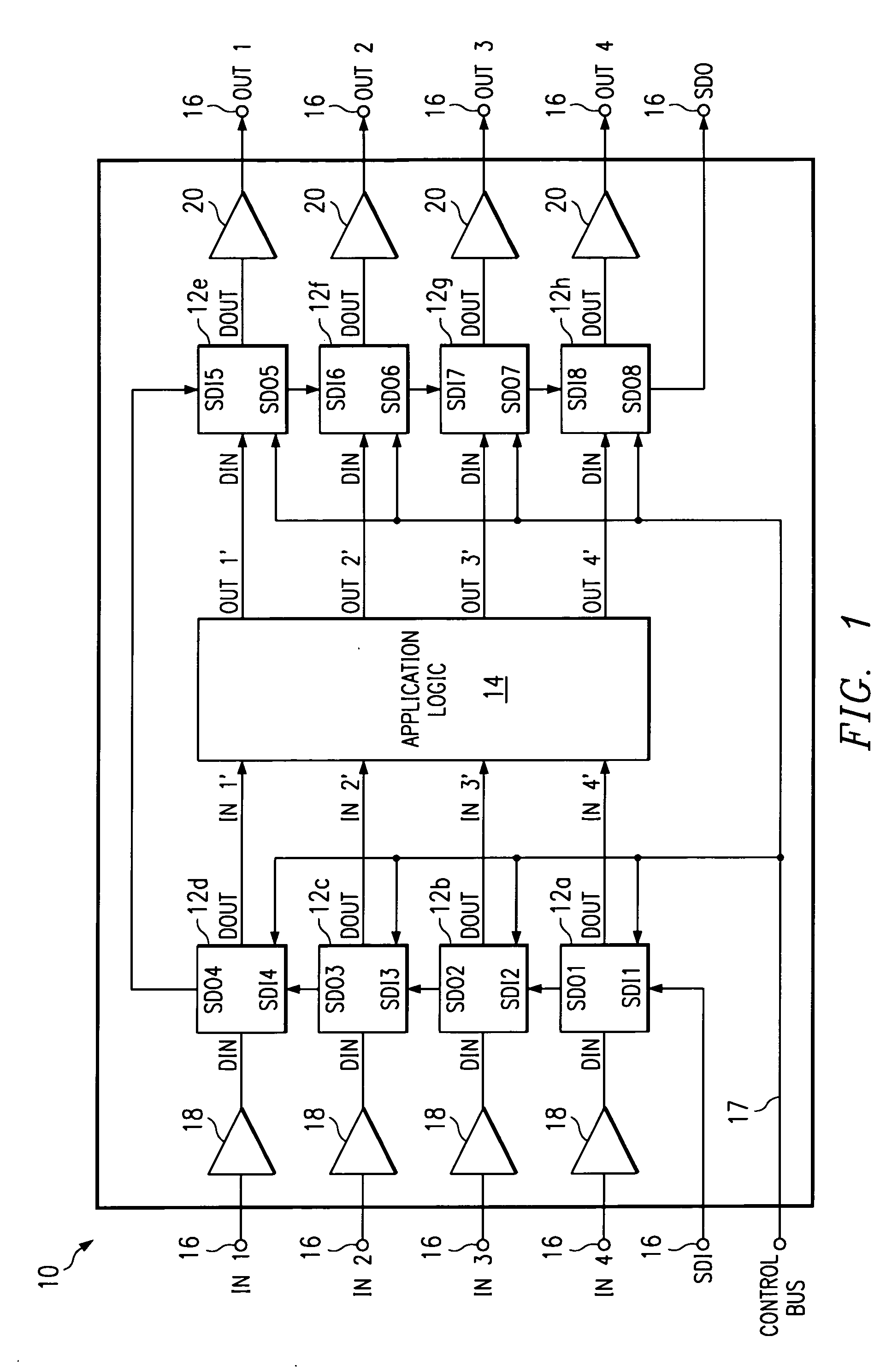
[0030] FIG. 1 illustrates a block diagram of an integrated circuit (IC) 10 having test cells 12a-h disposed about its boundary to control and observe data flow through the application logic 14 of the IC 10. The integrated circuit 10 comprises a plurality of pins 16 which provide an electrical connection between the integrated circuit 10 and other integrated circuits. For purposes of illustration, the integrated circuit 10 is shown with four pins receiving input signals, IN1, IN2, IN3 and IN4, and four pins providing output signals, OUT1, OUT2, OUT3 and OUT4. Other signals to the chip include a serial data input (SDI), a control bus 17, and a serial data output (SDO). The input signals IN1-IN4 are connected to input buffers 18 which output to respective test cells 12a-d. Each test cell ...


PUM


Abstract

A test cell (12) provides boundary scan testing in an integrated circuit (10) The test cell (12) comprises two memories, a flip-flop (24) and a latch (26), for storing test data. A first multiplexer (22) selectively connects one of a plurality of inputs to the flip-flop (24). The input of the latch (26) is connected to output of the flip-flop (24). The output of the latch (26) is connected to one input of a multiplexer (28), the second input to the multiplexer (28) being a data input (DIN) signal. A control bus (17) is provided for controlling the multiplexers (22, 28), flip-flop (24) and latch (26). The test cell allows input data to be observed and output data to be controlled simultaneously.

Description

RELATED APPLICATIONS[0001] This Application is related to co-pending Application for U.S. Pat. Ser. No. ______, filed ______, entitled "Testing Buffer / Register", incorporated herein by reference.[0002] This Application is related to co-pending Application for U.S. Pat. Ser. No. ______, filed ______, entitled "Enhanced Test Circuit", incorporated herein by reference.TECHNICAL FIELD OF THE INVENTION[0003] This invention relates in general to integrated circuits, and more particularly to a test cell used in an integrated circuit for providing a boundary scan test structure.BACKGROUND OF THE INVENTION[0004] Due to advances in the fields of board interconnect technology, surface mount packaging and IC density, board level testability is becoming increasingly complex. The combination of advanced board interconnect technology, such as buried wire interconnects and double-sided boards, along with surface mount packaging creates problems for in-circuit testing of the boards. In-circuit testi...

Claims


Application Information

Patent Timeline
IPC IPC(8): G01R31/28G01R31/3185G06F19/00
CPCG01R31/318555G01R31/318541
Inventor WHETSEL, LEE D. JR.
Owner WHETSEL LEE D JR
Learn More