
Semiconductor device

a semiconductor and integrated circuit technology, applied in the direction of transistors, solid-state devices, radiation controlled devices, etc., can solve the problems of high integration of lsi, reduced signal transmission amount, and restricted information processing of integrated circuits

Inactive Publication Date: 2004-10-07
SEMICON ENERGY LAB CO LTD
View PDF72 Cites 257 Cited by
  • Summary
  • Abstract
  • Description
  • Claims
  • Application Information

AI Technical Summary

Benefits of technology

The present invention relates to a technology for forming a three-dimensional integrated circuit on a glass substrate using a thin film semiconductor film. The invention aims to solve the problem of high integration in LSI and the resulting wiring resistance, delay, and energy consumption issues. The invention proposes a method of forming a thin film integrated circuit on a heat-resistant substrate and transferring it to another substrate to achieve higher performance and higher data rates. The invention provides a cost-effective solution for achieving high performance integrated circuits on a glass substrate.

Problems solved by technology

As the minimum dimension for LSI approaches a sub-micron region, a high integration of LSI has been limited.
Therefore, the delay of signals and the disturbance of waveforms occur, the amount of transmission of signals is decreased, and the performance of the information processing of the integrated circuit becomes restricted.
Moreover, as wirings are lengthened, a parasitic capacitance between the wirings is increased, and charging and discharging of energy to the wirings are also increased, thus electric power consumption cannot be lowered.
However, as the number of layers is increased so as to increase the amount of information to be processed by a semiconductor device, it becomes more difficult to interconnect each layer.
Therefore, when semiconductor elements are multilayered and the two layers are interconnected with more layers interposed therebetween, connection with a thin metal wire becomes difficult.
Further, the bonding with a thin metal wire is commonly performed in the vicinity of the edge of each layer, thus the area for connecting the thin metal wire is restricted and the number of terminals of each layer cannot be easily increased.
However, when two layers to be interconnected are separated from each other, the form of layers interposed between the two layers is restricted in order not to obstruct the connection with a solder ball, therefore, the flip chip bonding is unsuitable for multilayering as well as the wire bonding.
Accordingly, high integration of wirings is prevented and this is also unsuitable for mulilayering.
However, since the optical fiber is very expensive in general, it is not suitable for a semiconductor device using an integrated circuit in view of a cost thereof.
Thus, there are many restrictions on manufacturing steps, and it is difficult to form a thin film integrated circuit with a higher performance.
It is to be noted that in the case of stacking a plurality of organic resin, there is a threat that the plural organic resin is melted partially or is too adhesive when coated or baked.

Method used


Image

  • Semiconductor device
  • Semiconductor device
  • Semiconductor device

Examples


embodiment 1

[0139] In this embodiment, explanation is made on an example of forming a microprocessor by the use of a CPU (Central Processing Unit) formed of a plurality of thin film chips.

[0140] A TFT formed on a glass substrate operates at a lower rate as compared with a single crystalline transistor. Therefore, in the case of forming a CPU on a glass substrate, when the process contents become complex, it is difficult for a single CPU to carry out the processing at an adequate rate. To solve such problem, a series of processing steps of the CPU are divided into several steps in accordance with each purpose, and a CPU formed of one thin film chip is assigned to each processing step. Then, by interconnecting each thin film chip to each other by optical interconnect, a series of processing steps can be performed as is the case of using a single CPU. Each CPU formed of a thin film chip has only to perform the assigned processing step, thus, the operating rate is enhanced as compared with in perfo...

embodiment 2

[0150] The thin film integrated circuit according to the invention can be applied to various types of memories. By stacking memories, the capacitance of the memories can be enlarged while reducing the packaging area. In addition, by transmitting and receiving data between each thin film chip by means of optical transmission, the number of pins used for packaging can be reduced even in stacking the memories.

[0151] As a memory to be stacked, a RAM (volatile memory) as typified by an SRAM (Static Random Access Memory), a DRAM (Dynamic Random Access Memory) or the like, and a ROM (non-volatile memory) typified by a mask ROM, an EPROM (Erasable Programmable Read Only Memory), an EEPROM (Electrically Erasable Programmable ROM), a flash memory, a ferroelectric memory or the like can be utilized. Also, these memories may be combined to be stacked.

[0152] When stacking memories, a R / W (Read / Write) circuit for selecting reading or writing, a pre-charge circuit, a control circuit (refresh circu...

embodiment 3

[0163] In this embodiment, a configuration of a one-chip microcomputer formed of a plurality of thin film chips will be described.

[0164] FIG. 10 shows a block diagram of a microprocessor according to the invention. The microprocessor of the invention is formed of two layers of thin film chips. A thin film chip 630 on the first layer includes an SIO (Serial Input / Output) 631, an MMU (Memory Management Unit) 632, a counter 633, a DAC (Digital to Analog Converter) 634, a bus controller (bus interface) 635, an optical transmitting portion 636, and an input / output port 637. A thin film chip 640 on the second layer includes a CPU 641, a RAM 642, a ROM 643, and an optical transmitting portion 644.

[0165] The optical transmitting portions 636 and 644 each include a light emitting element and a light receiving element, and in the optical transmitting portions 636 and 644, various kinds of signals and power supply voltages are transmitted and received by optical transmission.

[0166] As describe...


PUM


Abstract

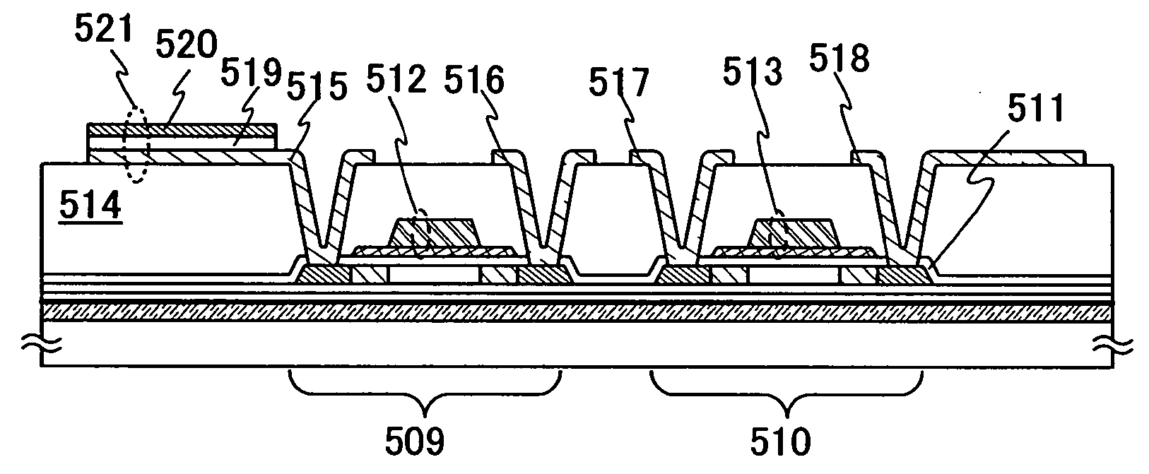
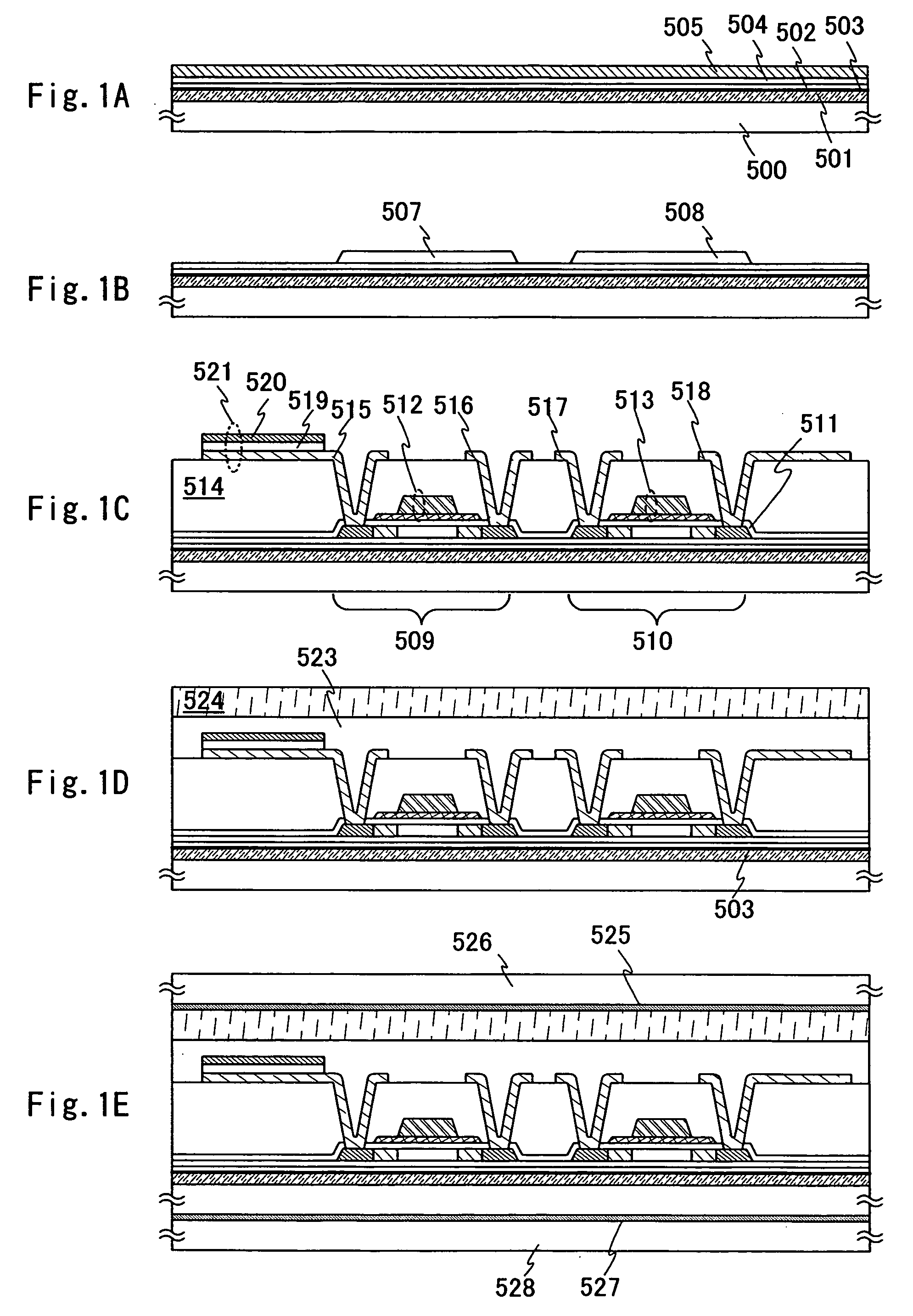
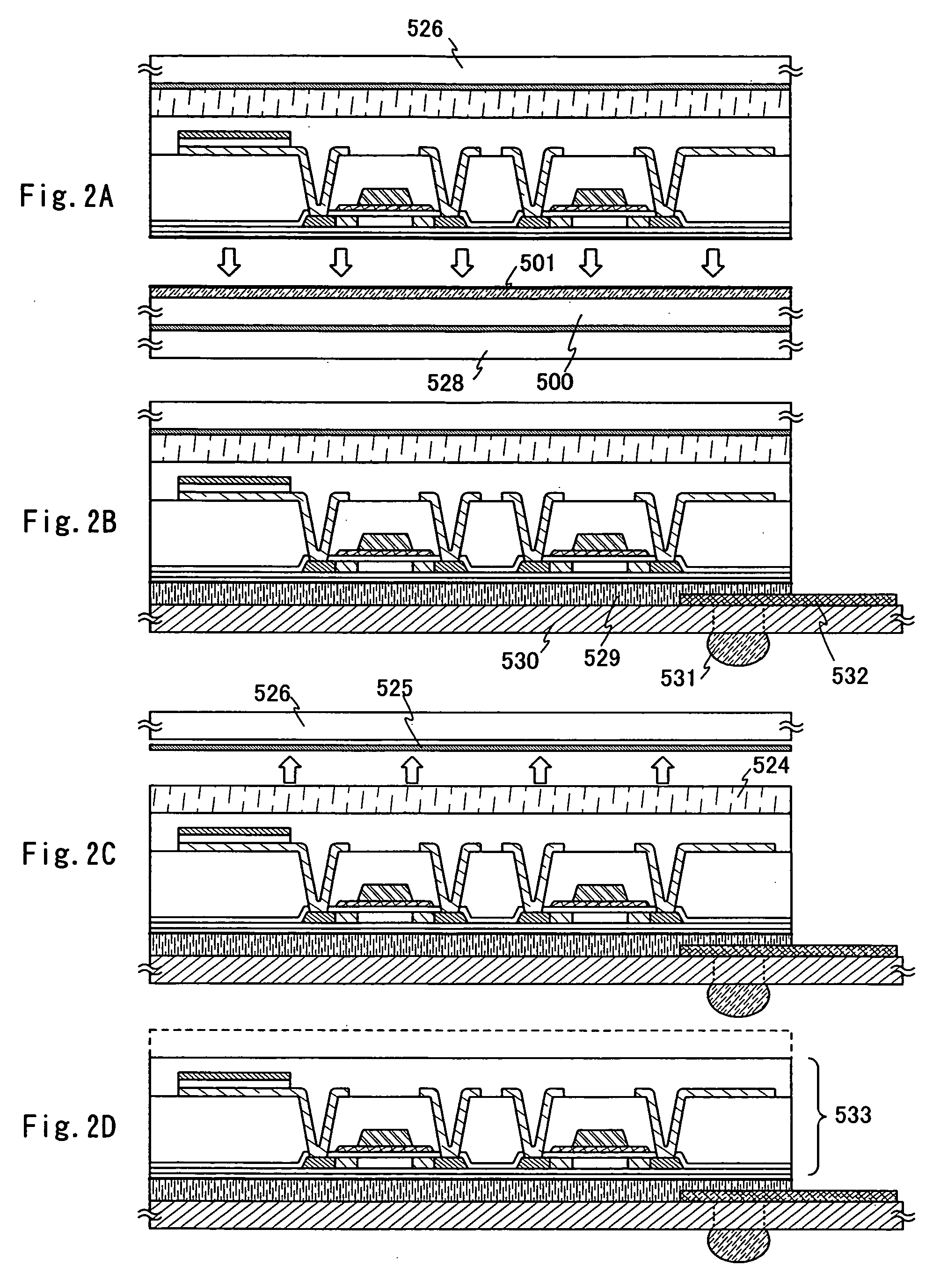
A semiconductor device which has a high performance integrated circuit formed of an inexpensive glass substrate and capable of processing a large amount of information and operating at higher data rates. The semiconductor device includes semiconductor elements stacked by transferring a semiconductor element formed on a different substrate. A resin film is formed between the stacked semiconductor elements and a metal oxide film is partially formed between the stacked semiconductor elements as well. A first electric signal is converted to an optical signal in a light emitting element electrically connected to one of the stacked semiconductor elements. Meanwhile, the optical signal is converted to a second electric signal in a light receiving element electrically connected to another one of the stacked semiconductor elements.

Description

[0001] 1. Field of the Invention[0002] The present invention relates to an integrated circuit (thin film integrated circuit) formed by using a semiconductor film which has a crystal structure and is formed on a glass substrate, and more particularly, the invention relates to a thin film integrated circuit in which a signal is transmitted by means of an optical interconnect, and to a semiconductor device using the relevant thin film integrated circuit.[0003] 2. Description of the Related Art[0004] As the minimum dimension for LSI approaches a sub-micron region, a high integration of LSI has been limited. In the case where a sufficient high integration is not realized in an integrated circuit, the wiring resistance is heightened. Therefore, the delay of signals and the disturbance of waveforms occur, the amount of transmission of signals is decreased, and the performance of the information processing of the integrated circuit becomes restricted. Moreover, as wirings are lengthened, a ...

Claims


Application Information

Patent Timeline
Patent Type & Authority Applications(United States)
IPC IPC(8): H01L21/02H01L27/146H01L21/77H01L21/822H01L21/84H01L27/00H01L27/06H01L27/12H01L27/15H01L27/32H01L29/786H01L31/12
CPCH01L21/8221H01L27/0688H01L27/1214H01L29/78621H01L27/3209H01L27/3227H01L29/78603H01L27/1266H10K59/32H10K59/60
Inventor KATO, KIYOSHITAKAYAMA, TORUMARUYAMA, JUNYAGOTO, YUUGOOHNO, YUMIKO
Owner SEMICON ENERGY LAB CO LTD
Learn More