Method for forming a photoresist pattern, method for forming a capacitor using the same and capacitor

Inactive Publication Date: 2004-03-11
SAMSUNG ELECTRONICS CO LTD
View PDF8 Cites 9 Cited by
  • Summary
  • Abstract
  • Description
  • Claims
  • Application Information

AI Technical Summary

Problems solved by technology

As the degree of integration of semiconductor devices increases, it becomes difficult to improve the capability of a capacitor because the horizontal area that the capacitor occupies decreases.
However, according to conventional methods for forming capacitors, additional processes may be necessary to vary the structure of a capacitor, thereby complicating the method for manufacturing the capacitor.
However, to realize a more highly integrated semiconductor device, a design rule thereof has been reduced, and an interval between storage electrodes of the semiconductor device has become even more miniscule.
As a result, there may be a limit for growing hemispherical silicon grains on storage electrodes.
Therefore, processing failures may occur during any of the complicated processes, and a productivity of the capacitor may be reduced.
However, according to the method, the height of a storage node electrode may not be increased because the low structure of the storage node electrode may be unstable.

Method used


Image

  • Method for forming a photoresist pattern, method for forming a capacitor using the same and capacitor
  • Method for forming a photoresist pattern, method for forming a capacitor using the same and capacitor
  • Method for forming a photoresist pattern, method for forming a capacitor using the same and capacitor

Examples


first embodiment

[0058] FIG. 2 illustrates a cross-sectional view of a capacitor according to the present invention.

[0059] Referring to FIG. 2, an insulation film 104 including contact plugs 102 is formed on a semiconductor substrate 100. The contact plugs 102 are electrically connected to a capacitor node contact region (for example, a source region of a transistor) of the semiconductor substrate 100 where an active region is defined. The contact plugs 102 are formed through the insulation film 104 formed on the substrate 100. At this time, the contact plugs 102 are regularly positioned on the substrate 100.

[0060] Storage node electrodes 106a having a cylindrical shape are formed on the insulation film 104. The storage node electrodes 106a are electrically connected to the contact plugs 102. Bottom faces of the storage node electrodes 106a are open. A portion of the bottom face of each of the storage node electrodes 106a makes contact with an upper face of each of the contact plugs 102.
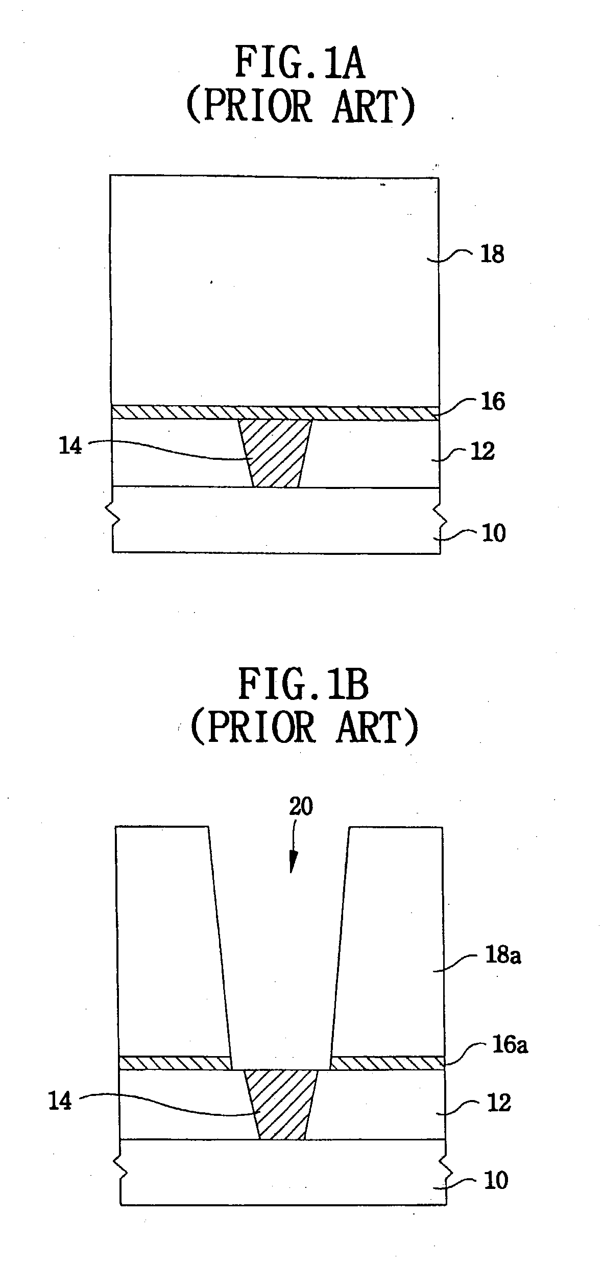
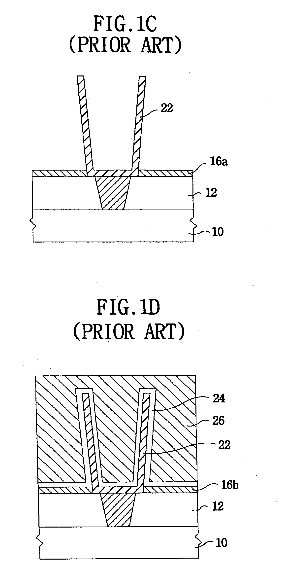
[0061] A die...

embodiment 2

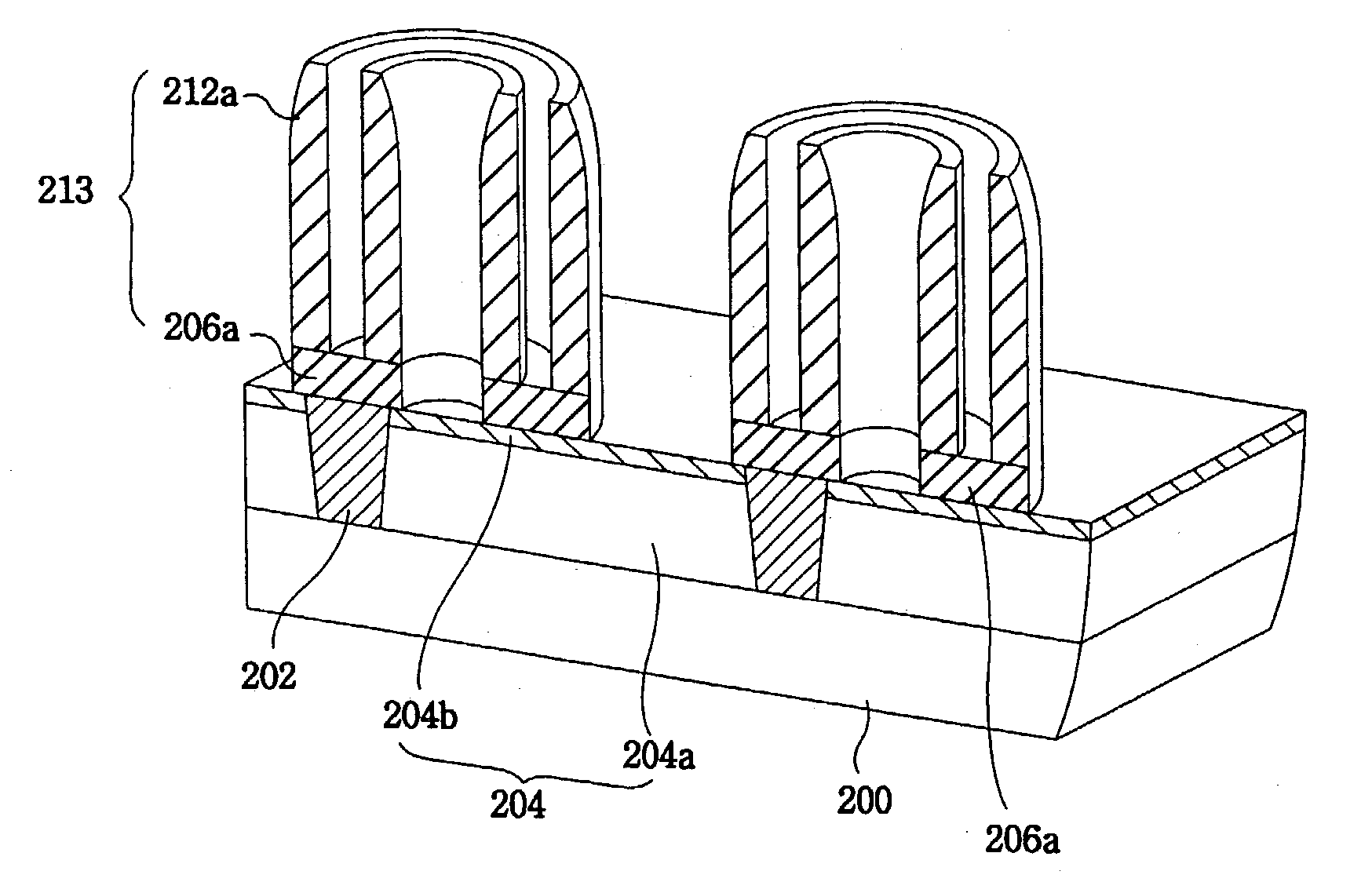
[0089] FIG. 8 illustrates a cross-sectional view of a capacitor according to a second embodiment of the present invention.

[0090] Referring to FIG. 8, an insulation film 204 including contact plugs 202 is formed on a semiconductor substrate 200. The insulation film 204 may include a composite film having an oxide film 204a and an etch stop film 204b sequentially formed on the oxide film 204a. The contact plugs 202 are regularly disposed on the semiconductor substrate 200.

[0091] Particularly, the insulation film 204 includes the contact plugs 202 electrically connected to a node contact region, for example, a source region of a transistor, of the semiconductor substrate 200 in which an active region is defined.

[0092] Ring-shaped pad polysilicon film patterns 206a electrically connected to the contact plugs 202 are formed on the contact plugs 202. A portion of each of the bottom faces of the ring-shaped pad polysilicon film patterns 206a makes contact with an upper portion of each of t...

embodiment 3

[0118] FIG. 10 illustrates a schematic plan view of a phase shift mask for cylindrical photoresist patterns according to a third embodiment of the present invention.

[0119] Referring FIG. 10, the phase shift mask includes first transmission regions 300a positioned along odd vertical lines and second transmission regions 300b disposed along even vertical lines. Positions of the first transmission regions 300a on a conventional X-axis of the phase shift mask are different from those of the second transmission regions 300. The first and second transmission regions 300a and 300b have rectangular shapes that have widths L.sub.1 of about 250 nm and heights L.sub.2 of about 200 nm. A first side of a transmission region is a distance L.sub.3 from a first side of an adjacent transmission region in the X-direction and a first side of a transmission region is a distance L.sub.4 from a first side of an adjacent transmission region in a conventional Y-direction. Distance L.sub.3 is about 500 nm a...


PUM


Abstract

In a method for forming a photoresist pattern, a method for forming a capacitor, and a capacitor manufactured using the same, a light is selectively irradiated onto a selected portion of a photoresist film formed on a substrate. An interfered light generated from the irradiated light is transmitted through other portions of the photoresist film except a ring-shaped portion of the photoresist film having a predetermined width along a boundary of the selected portion. The photoresist film is exposed using the interfered light and the light irradiated onto the selected portion. A cylindrical photoresist pattern having a minute width may be formed through developing the photoresist film. With the cylindrical pattern, the capacitor can be easily formed.

Description

[0001] 1. Field of the Invention[0002] The present invention relates to a method for forming a photoresist pattern, a method for forming a capacitor electrode using the same and a capacitor. More particularly, the present invention relates to a method for forming a ring-type photoresist pattern having an open bottom face and an open upper face, a method for forming a capacitor using the same, and a capacitor manufactured by using the ring-type photoresist pattern.[0003] 2. Description of the Related Art[0004] For functionality, semiconductor devices require fast operation and high accumulation capacity. For this purpose, manufacturing technologies for improving integration density, response speed and reliability are being developed.[0005] Dynamic random access memory (DRAM) is widely used as a semiconductor device that can input and output information. A DRAM has a cell region for storing information data in the form of electrons and a peripheral circuit region for transferring info...

Claims


Application Information

Patent Timeline
IPC IPC(8): G03F1/00G03F1/32G03F7/20G03F7/40H01G4/00H01L21/027H01G4/005H01G4/33H01G4/38H01L21/02H01L21/8242H01L23/522H01L27/02H01L27/108
CPCG03F1/14G03F1/32H01G4/005H01G4/33H01L21/0274H01L21/31144H01L28/91H01L23/5223H01L27/0207H01L27/10814H01L27/10817H01L27/10852H01L27/10855H01L21/32139H01L2924/0002G03F1/00H10B12/315H10B12/318H10B12/033H10B12/0335H01L2924/00H01L21/027
Inventor BAIK, IHN-GEE
Owner SAMSUNG ELECTRONICS CO LTD
Why Eureka
Try Eureka