Liquid crystal display panel and its manufacturing method
- Summary
- Abstract
- Description
- Claims
- Application Information
AI Technical Summary
Benefits of technology
Problems solved by technology
Method used
Image

Examples
eleventh embodiment
[0327] This first modified example is an example in which the invention is applied to a liquid crystal display panel being of an active matrix type using a thin film transistor (TFT) and having driving ICs provided on an FPC. An example in which the modification is applied to the eleventh embodiment will be described.
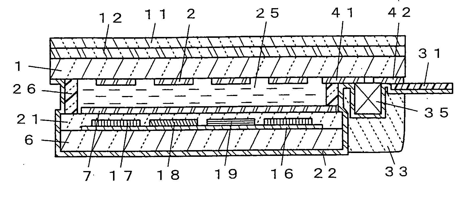
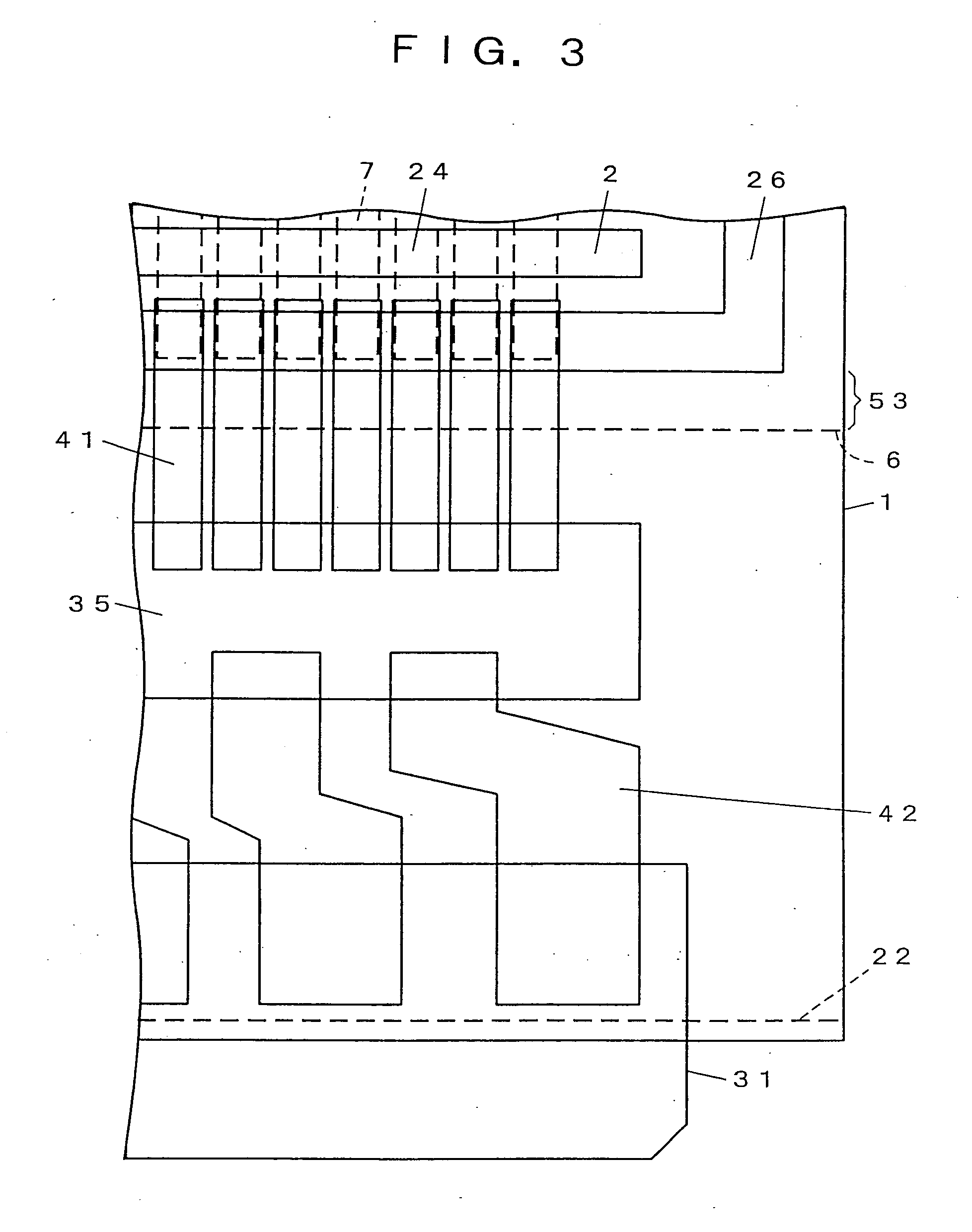
[0328] In this liquid crystal display panel, as shown in FIG. 38, a first substrate 1 is disposed on the lower side, and a second substrate 6 is disposed on the upper side in order to provide the TFT as a switching element on the first substrate 1. Further, on the first substrate 1, a gate electrode 81, a gate insulating film 82, and a semiconductor layer 83 are formed in this order, and further a source electrode 84 and a drain electrode 85 also serving as a display electrode are formed. Further, a semiconductor layer containing impurity ions (not shown) is provided between the source electrode 84 and the drain electrode 85 and the semiconductor layer 83. These constit...
second modified example
[0337] FIG. 39
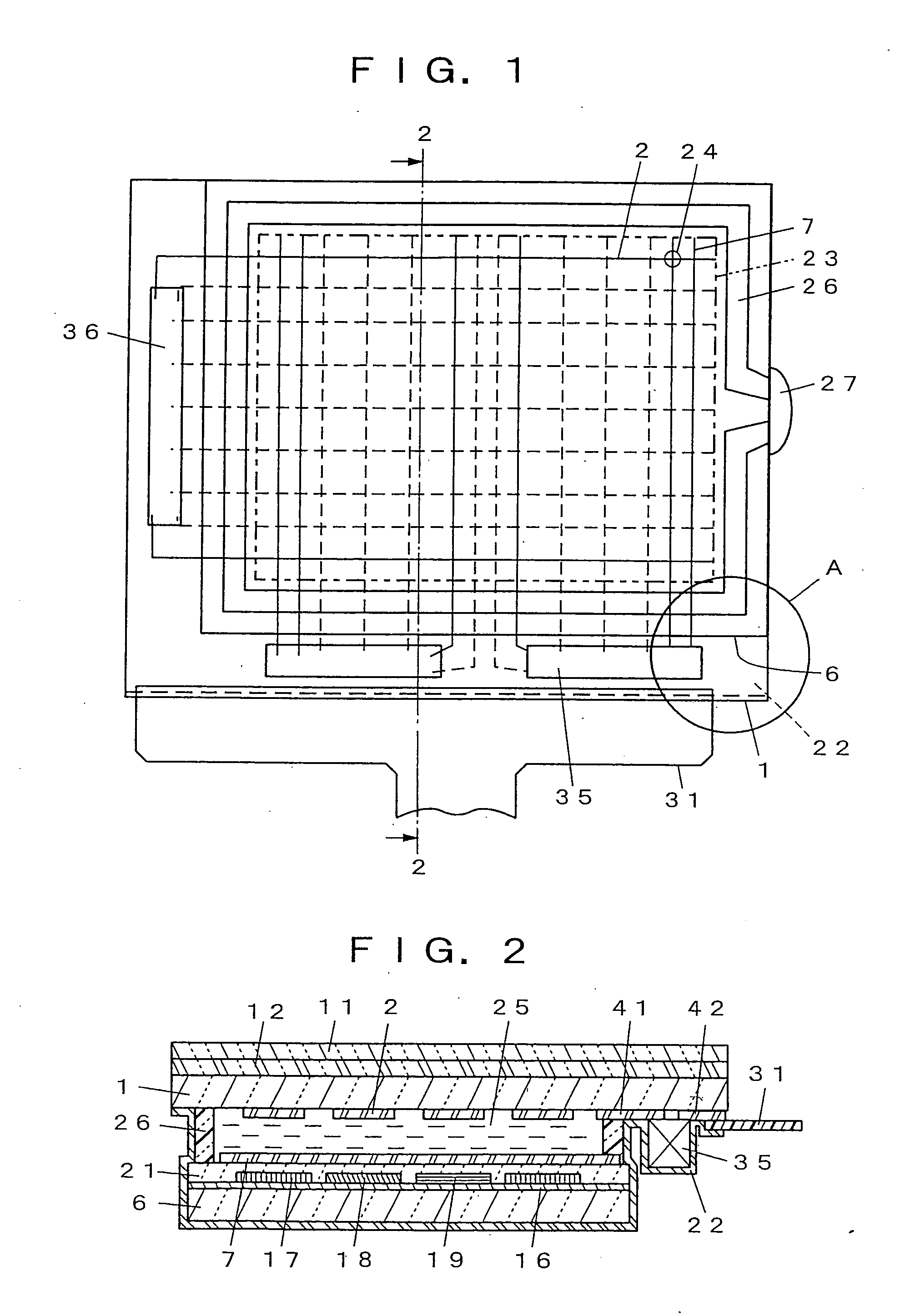
[0338] Next, a second modified example of each of the above-described embodiments will be described. FIG. 39 is a cross-sectional view, corresponding to FIG. 2, showing a cross section of the liquid crystal display panel of the modified example.
second embodiment
[0339] This second modified example is an example in which the invention is applied to a liquid crystal display panel having a configuration in which an FPC is directly connected to lead electrodes. FIG. 39 shows an example in which the modification is applied to the
[0340] The invention, as shown in FIG. 39, can also be applied to a liquid crystal display panel in which an FPC 31 is directly connected to a lead electrode 41 without mounting a driving IC on a first substrate, and the driving IC is separately provided via the FPC 31.
[0341] In the case shown in FIG. 39, it is preferable that a thin film insulating layer 22 is provided on the lead electrode 41 and on the FPC 31 to cover at least a portion of the lead electrode 41 outside a sealant 26, and further an insulating resin 32 is provided thereon. Even in such a configuration that the FPC 31 is directly connected to the lead electrode 41, there is no recognition of occurrence of electrolytic corrosion at the lead electrode 41 b...
PUM
 Abstract
Description
Claims
Application Information
 - R&D
- Intellectual Property
- Life Sciences
- Materials
- Tech Scout
- Unparalleled Data Quality
- Higher Quality Content
- 60% Fewer Hallucinations
Browse by: Latest US Patents, China's latest patents, Technical Efficacy Thesaurus, Application Domain, Technology Topic, Popular Technical Reports.
© 2025 PatSnap. All rights reserved.Legal|Privacy policy|Modern Slavery Act Transparency Statement|Sitemap|About US| Contact US: help@patsnap.com