
Adhesive sheet for producing semiconductor devices

Inactive Publication Date: 2003-10-09
TOMOEGAWA PAPER CO LTD
View PDF8 Cites 19 Cited by
  • Summary
  • Abstract
  • Description
  • Claims
  • Application Information

AI Technical Summary

Benefits of technology

[0010] The adhesive sheet has suitable elasticity and high adhesive strength when the adhesive layer is subjected to high temperatures. Therefore, the adhesive sheet of the present invention can prevent the generation of wire-bonding defects, mold flashes, and adhesive transfers, and this can thereby prevent the production of defective semiconductor devices.

Problems solved by technology

However, when this conventional adhesive sheet is used, in the wire-bonding step, there is a case in which a connection defect between the bonding wire and the lead is generated.
When a produced semiconductor device, in which the mold flash is generated, is mounted on a distributing board, because the filler resin attaches at the external connection parts of the lead, there is a possibility that connection defects are generated.
As a result, when the lead frame and the heat resistant film are cooled to room temperature, there is a possibility that warps are caused in the lead frame and the heat resistant film.
When warps are generated in the lead frame and the heat resistant film, in the resin filling step, it is impossible to mount the lead frame on positioning pins comprising a die, and there is a possibility that dislocation will occur.
In the wire-bonding step, the connection defect between the bonding wire and the lead is caused.
As this result, the lead frame easily vibrates and wire-bonding defects are easily generated.

Method used

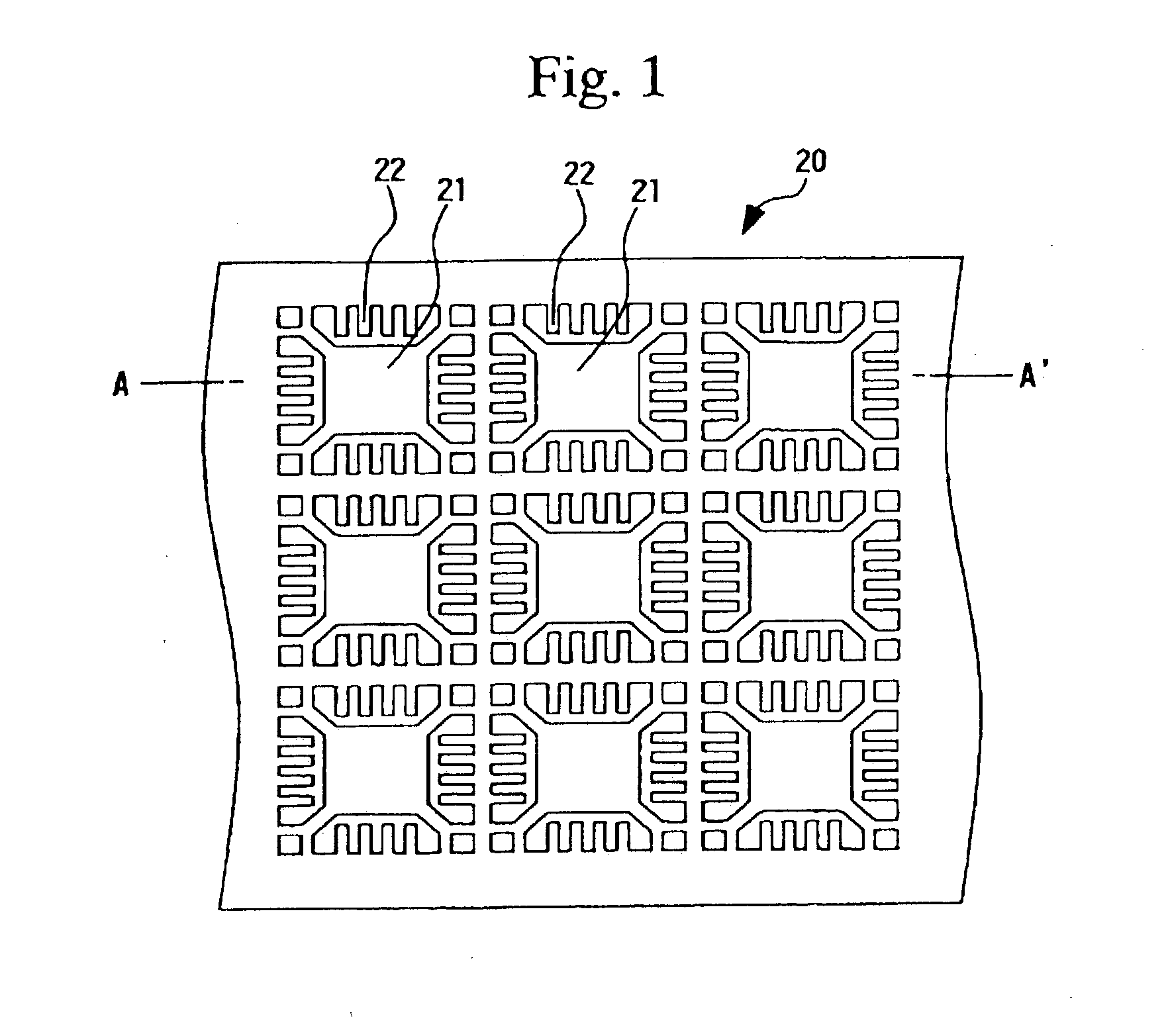
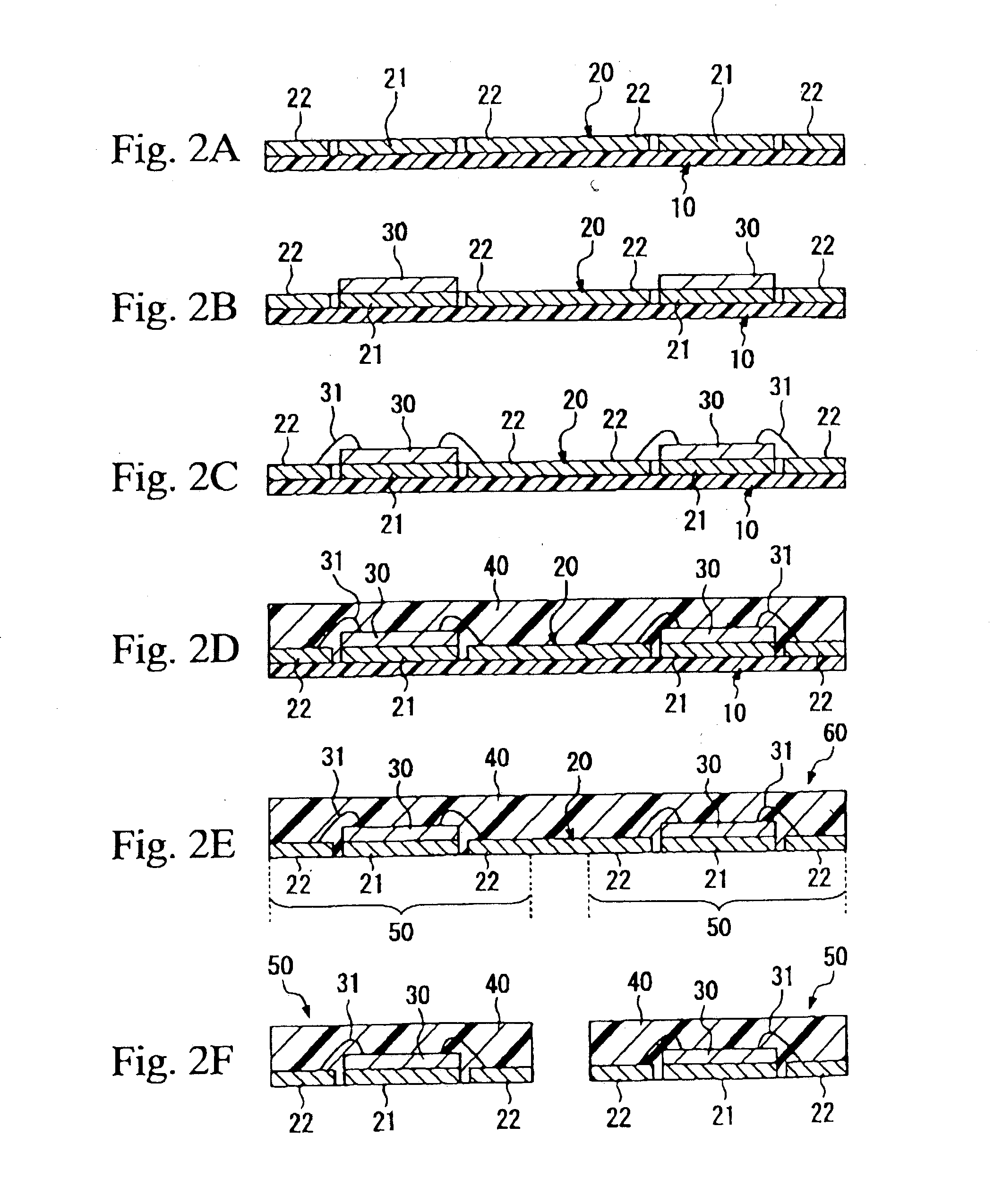

Image

  • Adhesive sheet for producing semiconductor devices
  • Adhesive sheet for producing semiconductor devices

Examples


example 2

[0051] The adhesive coating having the following composition of this Example was prepared.

[0052] Then, the adhesive sheet of this Example was prepared in a manner identical to that of Example 1, except that the adhesive coating of this Example was used. Moreover, the weight ratio of the thermosetting resin component (a) / the thermoplastic resin component (b) was 1.50.

2 The thermosetting resin component (a): Phenol resin 60 parts by weight The thermoplastic resin component (b) Dimer acid-based polyamide 40 parts by weight (weight average molecular weight: 12,000)

example 3

[0053] The adhesive coating having the following composition of this Example was prepared.

[0054] Then, the adhesive sheet of this Example was prepared in a manner identical to that of Example 1, except that the adhesive coating of this Example was used. Moreover, the weight ratio of the thermosetting resin component (a) / the thermoplastic resin component (b) was 1.43.

3 The thermosetting resin component (a): Maleimide resin (marketed by K-I Chemical 57 parts by weight Industry Co., Ltd.; and trade name: BMI-80) The thermoplastic resin component (b) Dimer acid-based polyamide 40 parts by weight (weight average molecular weight: 12,000) Other component Organic peroxides (marketed by NOF 3 parts by weight CORPORATION; trade name: Perbutyl P)

example 4

[0055] The adhesive coating having the following composition of this Example was prepared.

[0056] Next, as the heat resistant base, a copper foil (3 / 4 ounce; marketed by MITSUI MINING & SMELTING Co., Ltd.; trade name: 3EC-VLP; thickness: 25 .mu.m) was used. On a rough surface of the copper foil, the obtained adhesive coating was coated such that the thickness after drying was 8 .mu.m, and this was dried at 100.degree. C. for 5 minutes, and thereby the adhesive sheet of this Example was obtained. Moreover, the weight ratio of the thermosetting resin component (a) / the thermoplastic resin component (b) is 1.48.

4 The thermosetting resin component (a): Epoxy resin (marketed by Japan Epoxy Resins Co., 30 parts by weight Ltd., trade name: YX-4000H; epoxy equivalent: 190) Phenol resin (marketed by SHOWA 29 parts by weight HIGHPOLYMER; trade name: CKM-2400) The thermoplastic resin component (b) Dimer acid-based polyamide (weight average 40 parts by weight molecular weight: 12,000) Other compo...


PUM

PropertyMeasurementUnit
Pressureaaaaaaaaaa
Angleaaaaaaaaaa
Angleaaaaaaaaaa

Abstract

An adhesive sheet for producing semiconductor devices, such as QFNs, can prevent the generation both of wire-bonding defects and mold flashes, and can thereby prevent the production of defective semiconductor devices. The present invention provides an adhesive sheet for producing semiconductor devices which is detachably attached to a lead frame and which comprises a heat resistant substrate and an adhesive layer which is arranged on one surface of the heat resistant substrate, wherein the adhesive layer contains, a thermosetting resin component (a) and a thermoplastic resin component (b); and the weight ratio of the component (a) / the component (b) is 0.3 to 3.

Description

[0001] 1. Field of the Invention[0002] The present invention relates to an adhesive sheet which is detachably attached to a lead frame and which is used for producing semiconductor devices, such as quad flat non-leaded type semiconductor packages.[0003] 2. Description of the Related Art[0004] Recently, with the reduction in size of electronics, such as portable personal computers and portable telephones, and increasing functions thereof, it has been desired to reduce the size of electronic elements comprising electrorics, so as to allow integration in high density. That is, a technique for mounting electronic elements in high density has been required. In light of the above, instead of a peripheral-mounting type semiconductor device in which external terminals are mounted at a peripheral area of a semiconductor device, such as a QFP (Quad Flat Package) and a SOP (Small Out Line Package), a surface-mounting type semiconductor device in which external terminals are mounted at a surfac...

Claims


Application Information

Patent Timeline
IPC IPC(8): B32B7/10B32B15/08
CPCB32B7/10Y10T428/28H01L24/97H01L2224/48091H01L2224/97H01L2924/01004H01L2924/01005H01L2924/01012H01L2924/01013H01L2924/01015H01L2924/0102H01L2924/01025H01L2924/01027H01L2924/01029H01L2924/0103H01L2924/01032H01L2924/01033H01L2924/0104H01L2924/01042H01L2924/01046H01L2924/01047H01L2924/01049H01L2924/01051H01L2924/01074H01L2924/01078H01L2924/01079H01L2924/01082H01L2924/04941H01L2924/14B32B15/08Y10T428/2804H01L2224/85207H01L2224/85205H01L24/45H01L2924/15747H01L2224/48247H01L2224/45144H01L2924/01024H01L2924/01019H01L2924/01006H01L2224/85H01L2924/00014H01L2924/20303H01L2924/00H01L2924/20305H01L2924/181H01L2924/20304H01L2924/00012H01L23/48
Inventor NAKABA, KATSUJINAKAJIMA, TOSHIHIROSATO, TAKESHIOKA, OSAMU
Owner TOMOEGAWA PAPER CO LTD
Learn More