
Method for forming a dielectric film

a dielectric film and film technology, applied in the manufacture of electrode systems, solid-state diffusion coatings, electric discharge tubes/lamps, etc., can solve the problems of large air gap, large size of bubbles (or air gaps) in the dielectric film, and high cost of obtaining dielectric films

Inactive Publication Date: 2003-01-16
PANASONIC CORP
View PDF2 Cites 0 Cited by
  • Summary
  • Abstract
  • Description
  • Claims
  • Application Information

AI Technical Summary

Benefits of technology

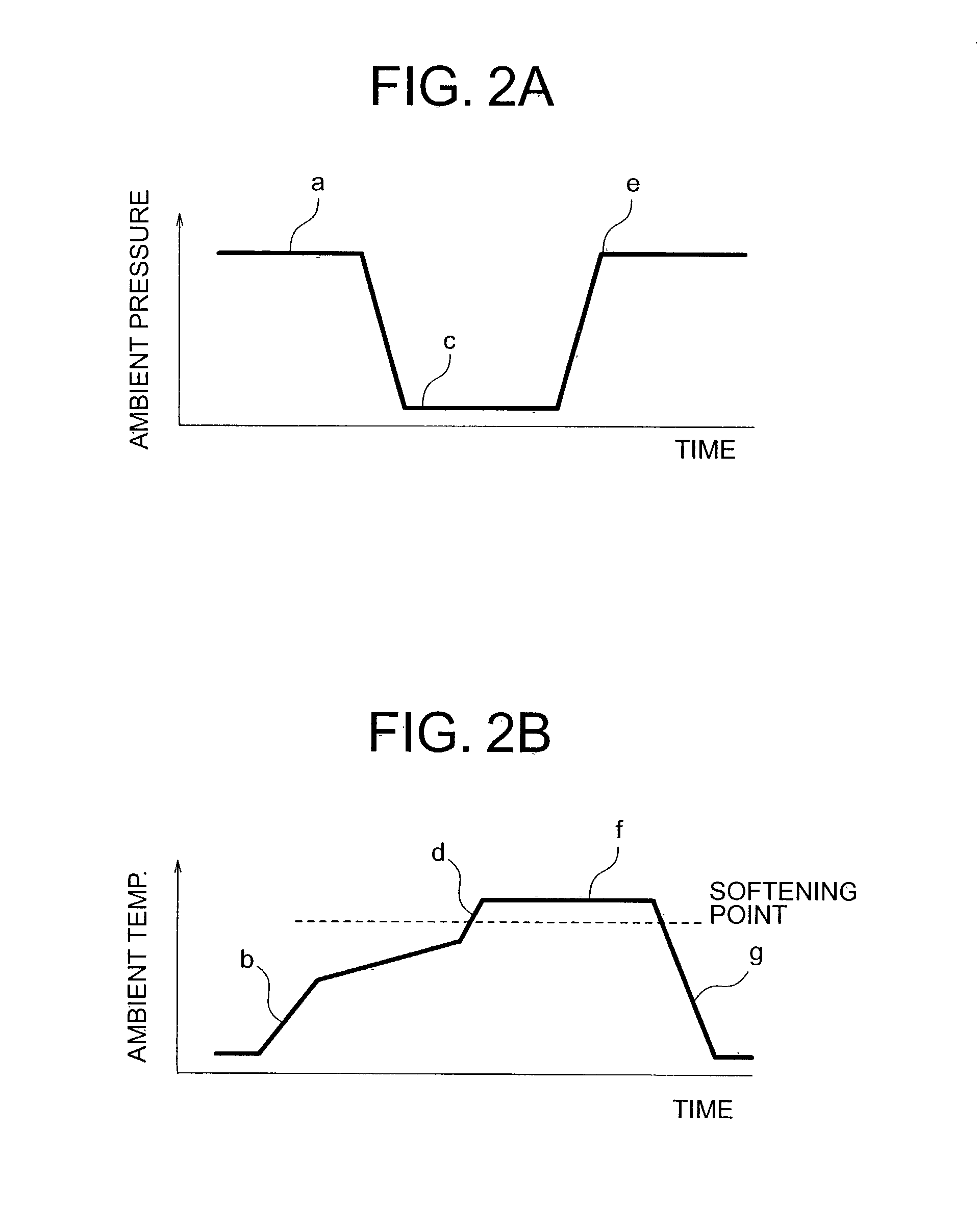
[0013] In accordance with the method and system of the present invention, the number of the bubbles (gas bubbles or air gaps) formed in the resultant dielectric film can be reduced by the reduced ambient pressure, and the dimensions of the bubbles remaining in the insulating film after reduction of the ambient pressure can be reduced by the step of increasing the reduced ambient pressure. Thus, the number and the dimensions of the bubbles can be reduced in the resultant dielectric film, whereby the resultant dielectric film has excellent film properties such as higher withstand voltage, higher density and higher transparency.

Problems solved by technology

In the described technique, if the dielectric powder is subjected to the baking at a lower ambient temperature and thus at a lower fluidity thereof, the degassing effect is relatively limited.
However, this involves a lower throughput and higher costs for obtaining the dielectric film.
In addition, the lower fluidity may leave bubbles (or air gaps) having large dimensions in the resultant dielectric film due to the reduced pressure which generally expands the bubbles in the molten dielectric material.
Further, if reduction of the transparency is associated with generation of the bubbles, the resultant PDP has a poor brightness in the discharge thereof.

Method used


Image

  • Method for forming a dielectric film
  • Method for forming a dielectric film
  • Method for forming a dielectric film

Examples


first embodiment

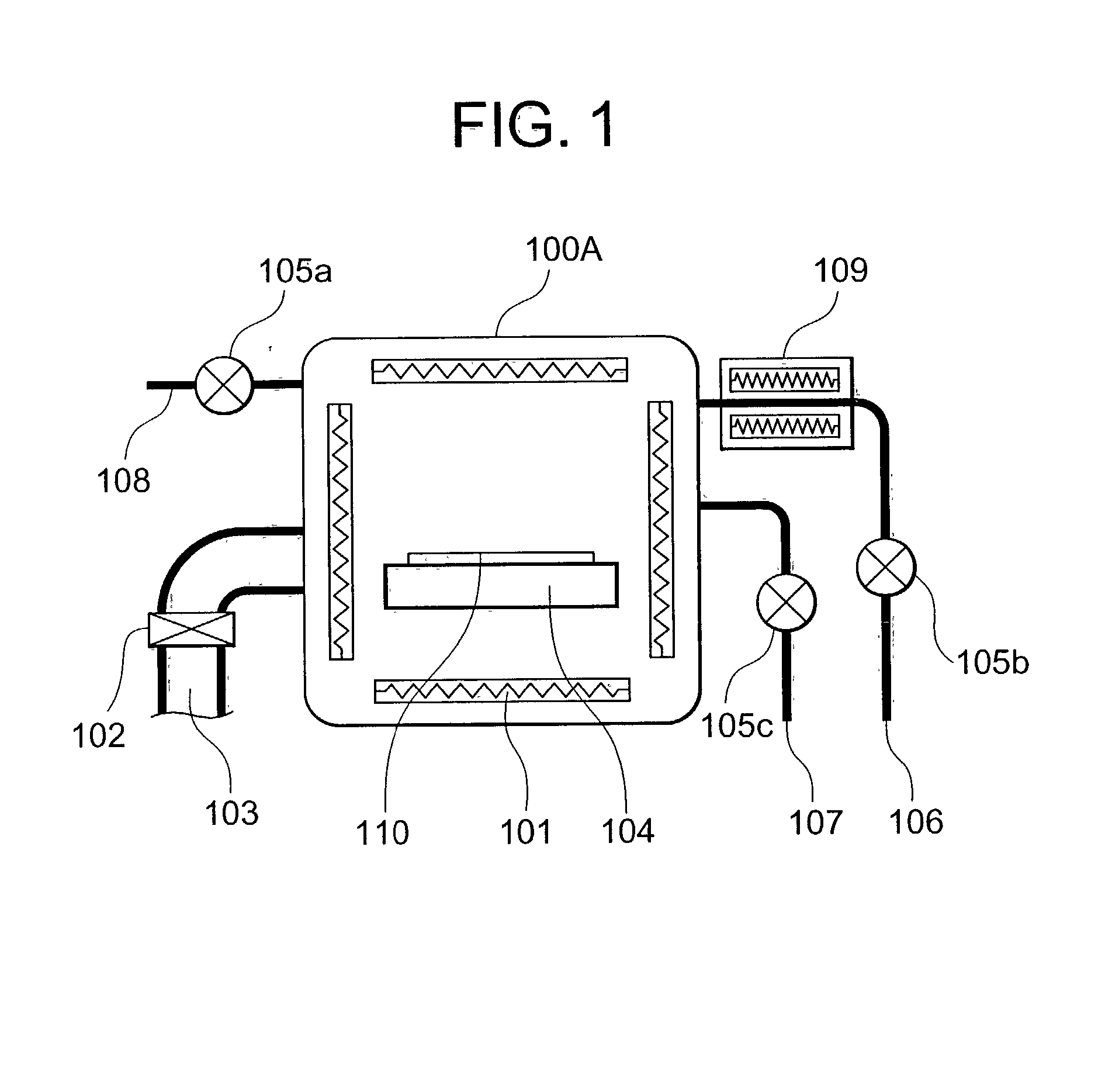
[0022] Referring to FIG. 1, a system for forming a dielectric film according to the present invention includes a batch-type baking furnace 100A receiving therein a mounting table 104 which mounts thereon a substrate 110 and has four heaters 101 surrounding the mounting table 104. The baking furnace 100A is connected with an exhaust system 103 including an exhaust gate valve 102, a leakage system system 108 including a gas valve 105a, a gas re-introduction system 106 including a gas valve 105b and a gas heater 109, and a gas introduction system 107 including a gas valve 105c.

[0023] Referring to FIGS. 2A and 2B, there are shown an ambient pressure profile and an ambient temperature profile used in the system of FIG. 1 for forming a dielectric film on the substrate 110. First, paste including dielectric powder is applied onto the substrate 110, followed by placing the substrate 110 on the mounting table 104. Subsequently, the temperature in the furnace 110A is raised as denoted by (b) ...

second embodiment

[0028] Referring to FIG. 3, a system for forming a dielectric film according to the present invention includes a belt-type inline baking furnace 100B which is associated with a substrate carriage system 111. The inline baking furnace 100B includes a heating chamber 120 for heating the substrates 110 at an atmospheric pressure, a load-locked replacement chamber 130, a baking chamber 140 for baking the substrates at a reduced pressure, a load-locked replacement chamber 150, and a cooling chamber 160, which are arranged in this order along the direction in which the substrate carriage system 111 transfers the substrates 110. The replacement chamber 130 has an inlet gate 131 and an outlet gate 132, whereas the replacement chamber 150 has an inlet gate 151 and an outlet gate 152.

[0029] The replacement chamber 130 is connected with an exhaust system 103a including an exhaust gate valve 102a, a gas re-introduction system 106a including a gas valve 105d and a gas heater 109a, and a gas intr...


PUM

PropertyMeasurementUnit
thicknessaaaaaaaaaa
pressureaaaaaaaaaa
pressureaaaaaaaaaa

Abstract

A method for forming a dielectric film in a PDP includes the steps of: reducing the ambient pressure of an insulating film including a dielectric material before the ambient temperature reaches the reaction temperature of the dielectric material; introducing heated gas to increase the ambient pressure up to the atmospheric pressure while maintaining the ambient temperature at the reaction temperature; and lowering the ambient temperature down to the solidifying temperature of the insulating film while maintaining the atmospheric ambient pressure.

Description

[0001] (a) Field of the Invention[0002] The present invention relates to a method for forming a dielectric film and, more particularly, to a method for forming a dielectric film having a relatively large thickness and a relatively large area. The present invention also relates to a system for forming a dielectric film on a substrate.[0003] (b) Description of the Related Art[0004] A plasma display panel (PDP) is known as a flat display panel especially suited to achieving a large screen, and generally used in a personal computer, a work station, or a wall TV.[0005] A PDP has a front panel and a rear panel sandwiching therebetween a plurality of phosphors, a plurality of sustaining electrodes and a thick dielectric film, wherein the phosphors are formed on the rear panel and the sustaining electrodes and the thick dielectric film are consecutively formed on the front panel. In order to form the thick dielectric film on the front panel, paste including powder of a dielectric material i...

Claims


Application Information

Patent Timeline
Patent Type & Authority Applications(United States)
IPC IPC(8): C03C17/00C23C10/28C23C24/10C23C26/02H01J9/02H01J11/22H01J11/34H01J11/38
CPCC03C17/001C23C10/28C23C24/10C23C26/02H01J9/02H01J2211/38
Inventor YOSHIOKA, TOSHIHIROMIYAKOSHI, AKIRA
Owner PANASONIC CORP
Learn More