
MEMS actuator with lower power consumption and lower cost simplified fabrication

a technology of micro-actuators and actuators, applied in the direction of generators/motors, optical elements, conductive pattern formation, etc., can solve the problems of not always a suitable or ideal material for every application of micro-actuators, brittleness and subject to breaking, and brittleness limits devices, especially actuators, so as to achieve less precise and reduce the loss of device performance.

Inactive Publication Date: 2002-09-12
HONEYWELL INT INC
View PDF16 Cites 15 Cited by
  • Summary
  • Abstract
  • Description
  • Claims
  • Application Information

AI Technical Summary

Benefits of technology

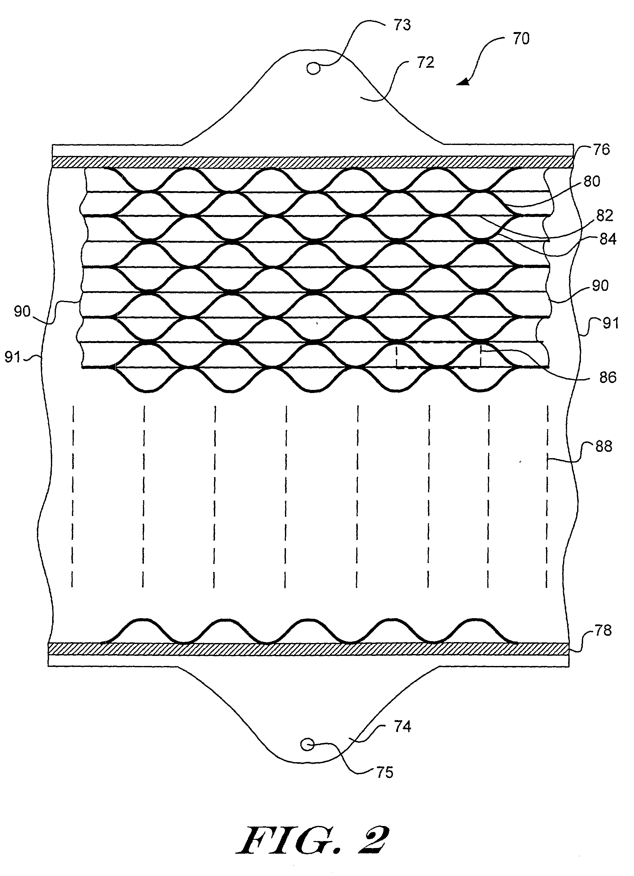
[0008] The sheets included in the present invention require only a single electrode layer bonded or applied to a substrate layer. The electrode layer is preferably formed of a conductor material deposited over the substrate layer, and a dielectric material deposited over the conductor. The substrate layer may be a polymer, ceramic, silicon, steel, or any other material that provides the desired characteristics for a particular application. The first and second sheets of each pair can be bonded together so that the front surfaces of the sheets are in close proximity to one another near the bonded regions. The close proximity of the sheets helps overcome the initial separation of the non-bonded regions of the sheets, and zip together inward from the bonding locations toward the center of the non-bonded regions. The attraction of the sheets for each other upon the application of an electrical potential provides the force for the microactuator.
[0009] In one method of manufacture, the sheet pairs are formed by first bonding together the sheets at periodic intervals, for example, along regularly spaced parallel lines. This can be done using manufacturing techniques such as heat bonding or adhesive application. With the sheet pairs formed, the sheet pairs can be bonded together many at a time, to form the microactuator array. The process of bonding together the multiple, already formed sheet pairs can be less precise with little or no loss in device performance than the process used to bond the sheets of a sheet pair. Since no voltage is applied between the sheet pairs, the distance between the sheet pairs may not be as critical as the distance between the sheets forming each pair.

Problems solved by technology

Despite the many favorable attributes of silicon, it is not always a suitable or ideal material for every application of MEMS.
Silicon is brittle and subject to breaking, particularly as the total device size increases.
This brittleness limits devices, especially actuators, to relatively small sizes capable of only small displacements and forces.
The shapes that can be realized in silicon are typically restricted by crystalline planes or 2-D fabrication processes, and more complicated structures often result in prohibitively high cost and low yield.

Method used


Image

  • MEMS actuator with lower power consumption and lower cost simplified fabrication
  • MEMS actuator with lower power consumption and lower cost simplified fabrication
  • MEMS actuator with lower power consumption and lower cost simplified fabrication

Examples


Embodiment Construction

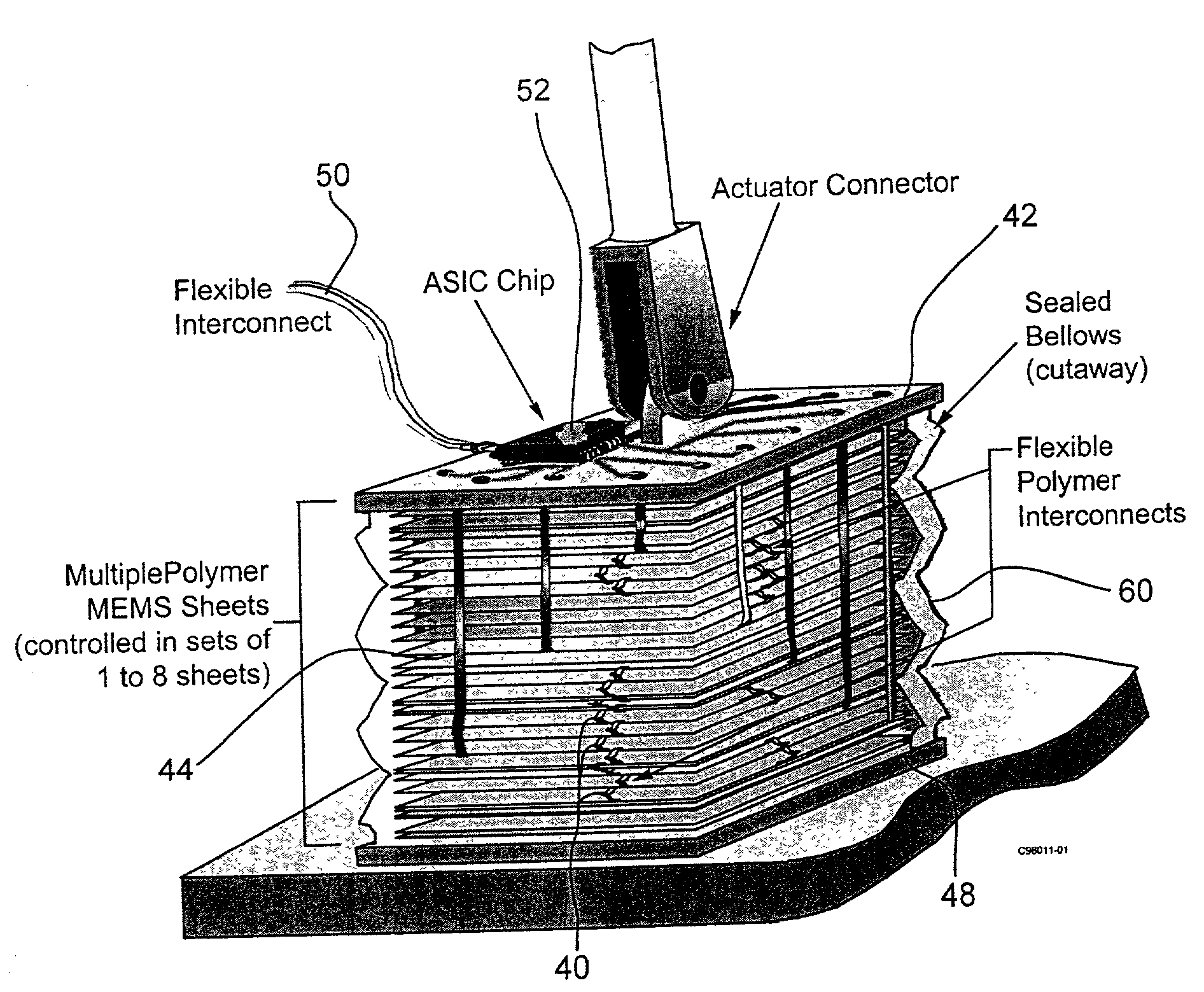
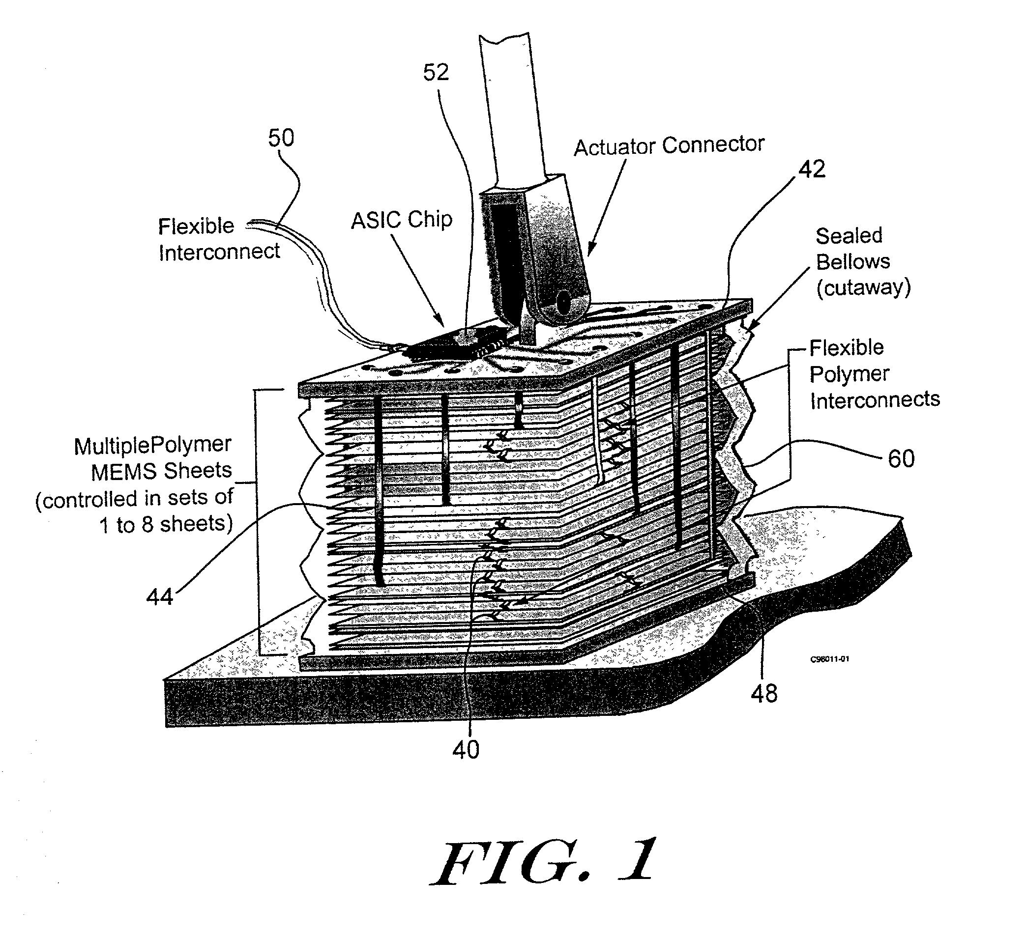
[0020] FIG. 1 is a partial cut-away perspective view of a microactuator using polymer sheets. The illustrative microactuator is formed by stacking and bonding together multiple polymer sheets, as described in for example, co-pending U.S. patent applications: Ser. No.______ to Cabuz et al., filed Dec. 29, 1999, entitled "POLYMER MICROACTUATOR ARRAY WITH MACROSCOPIC FORCE AND DISPLACEMENT", and U.S. patent application Ser. No. 09 / 476,667 to Homing, filed Dec. 30, 1999, entitled "MICROACTUATOR ARRAY WITH INTEGRALLY FORMED PACKAGE", both of which are incorporated herein by reference.

[0021] As described in the above references, electrodes from selected sheets can be electrically tied together or can be individually addressed, depending on the degree of control and sophistication of the end use, noting that individual addressing requires more connections, so it would involve higher cost but finer control when needed. Electrical contact between layers and sheets can be made through flexibl...


PUM

PropertyMeasurementUnit
Lengthaaaaaaaaaa
Forceaaaaaaaaaa
Pressureaaaaaaaaaa

Abstract

A microactuator device is disclosed that includes a plurality of generally parallel thin flexible sheets bonded together in a predetermined pattern to form an array of unit cells. Preferably, each of the sheets has only a single electrode layer located on one side of the sheet. Pairs of such sheets are then bonded together at spaced bonding locations with the electrode layers facing one another. Several sets of such sheet pairs can then be bonded together to form a microactuator device.

Description

RELATED APPLICATIONS[0001] This Application is related to co-pending U.S. patent application Ser. No. ______ to Cabuz et al., filed Dec. 29, 1999, entitled "POLYMER MICROACTUATOR ARRAY WITH MACROSCOPIC FORCE AND DISPLACEMENT"; and to co-pending U.S. patent application Ser. No. 09 / 476,667 to Homing, filed Dec. 30, 1999, entitled "MICROACTUATOR ARRAY WITH INTEGRALLY FORMED PACKAGE", both of which are incorporated herein by reference.FIELD OF THE INVENTION[0003] The present invention relates to microactuators having macroscopic force and displacement. More particularly, the invention relates to microactuators comprising a 3-D array of small actuator cells, which are formed from stacked substrate sheets having an electrode layer on only one side of the substrate sheet.BACKGROUND OF THE INVENTION[0004] Most microactuator arrays, used as MEMS (Micro-Electro-Mechanical-S- ystems) devices, are fabricated in silicon. Despite the many favorable attributes of silicon, it is not always a suitab...

Claims


Application Information

Patent Timeline
IPC IPC(8): B81B3/00B81B7/04H02N1/00
CPCB81B3/0021B81B2203/0315B81B2203/04B81B2207/07B81C2201/019H02N1/006Y10T29/49128Y10T29/49005Y10T29/49155Y10T156/1025Y10T29/49146Y10T29/42
Inventor HORNING, ROBERTJOHNSON, BURGESS
Owner HONEYWELL INT INC
Learn More