
Circuit component

a technology of circuit components and components, applied in the field of circuit components, can solve the problems of poor mechanical strength of metal sheets thinner than 0.1 mm, deterioration factor in characteristics, and difficulty in machining

Inactive Publication Date: 2002-08-08
PANASONIC CORP
View PDF12 Cites 7 Cited by
  • Summary
  • Abstract
  • Description
  • Claims
  • Application Information

AI Technical Summary

Benefits of technology

[0011] A structure in accordance with the present invention is advantageous in preventing a possible deterioration in the electrical conduction between the second circuit board and the joint circuit board which would be caused by repeated heat cycles. Thus the present invention offers a circuit component that provides stable operating characteristics for a long operating period.

Problems solved by technology

The difference in the coefficients of thermal expansion creates a substantial stress in a material (a solder, for example) coupling the spacer 4 and the electrode, resulting in micro-cracks or the like problems in the coupling material and causes an electrical connection trouble between the coupling board 3 and the circuit board 1.
This is a deteriorating factor in the characteristics.
The metal sheets thinner than 0.1 mm are poor in the mechanical strength; as a result, even a small external force can make a terminal 8 deformed, or machining difficulties would arise.
On the other hand, the metal sheets thicker than 0.5 mm will have too much rigidity, which would have the same problem as observed in the conventional dielectric filters.
A high count of terminals 8 means an increased number of process steps in assembly operation, which impairs the manufacturing productivity.
On the other hand, the gap H greater than 5 mm makes height of a dielectric filter itself great, that does not fit to the downsizing objective for an electronic apparatus.
On the other hand, a length M greater than 80 mm leads to a bulky-sized dielectric filter, which is not suitable to the downsizing objective for an electronic apparatus.

Method used


Image

  • Circuit component
  • Circuit component
  • Circuit component

Examples


second embodiment

[0070] A second exemplary embodiment of the present invention is described with reference to FIG. 8 and FIG. 9.

[0071] The difference with the structure of FIG. 3 is that a terminal 8 in the present embodiment has a T-shaped form at the connection section 8b. Or, the end of connection section 8b is branched towards opposite directions, and each end part of the branch makes contact with electrode 1a of the circuit board 1.

[0072] It is preferred that respective ends of the branched connection section 8b are provided with a bent section 8i, as shown in FIG. 8. When a terminal 8 is connected to an electrode 1a using a bonding material 9, the bent section 8i helps the bonding material 9 form a fillet along the side face of bent section, preventing it from spreading over the electrode 1a. As a result, the area of bonding material 9 can be limited to be small.

[0073] In place of the above-described bent section, a protrusion may be provided at the end of the branched connection section 8b.

[0...

third embodiment

[0076] A third exemplary embodiment of the present invention is described with reference to the drawings FIG. 10 and FIG. 11.

[0077] Referring to FIG. 10 and FIG. 11, a terminal 8 is provided with one connection section 8a, which is stretching from the joint section 8e, and a pair of opposing sections 8d stretching from the joint section 8e to oppose the connection section 8a. Namely, the terminal 8 in the present embodiment is based on the structure of FIG. 3, and is provided with an increased number of opposing sections 8d, the connection section 8a is being disposed to be locating above the clearance formed by the pair of the opposing sections 8d.

[0078] In the configuration of FIG. 3, part of the elastic section 8c is utilized to work also as the opposing section 8d. So, the elastic section 8c has a curved form. On the other hand, the elastic section 8c in the present embodiment is straight-formed, as shown in FIG. 10 and FIG. 11, and the elastic section 8c and the connection sect...

fourth embodiment

[0082] A fourth exemplary embodiment of the present invention is described referring to FIG. 13 through FIG. 15.

[0083] The terminal 8 in the present embodiment comprises an elastic section 8c disposed between the connection section 8a and the connection section 8b. The present terminal 8 is not designed to hold a coupling board 3. The end portion of the connection section 8a is bent inward towards the connection section 8b so that it does not damage the electrodes and other elements.

[0084] In a terminal 8 of the present embodiment, the connection section 8a and the connection section 8b are disposed substantially in parallel to each other, and the elastic section 8c is disposed slant to the connection sections 8a and 8b.

[0085] The connection section 8a is attached to an electrode disposed on the reverse-surface of the coupling board 3, while the connection section 8b is attached to the electrode la disposed on the circuit board 1. The terminals 8 provides an effective elastic proper...


PUM


Abstract

A circuit component comprising a circuit board and a terminal for mounting the circuit board on a second circuit board. A length of the circuit board is 10 mm-80 mm, a difference in a coefficient of thermal expansion between the circuit board and the second circuit board is or 0.2x10⁻⁵ / ° C. greater. The terminal is made of an elastic material, and comprised of a first connection section, a second connection section and an elastic section disposed between the first and second connection sections. and the terminal separates the circuit board from the second circuit board by 0.3 mm-5 mm. In the circuit components of the present invention, deterioration in the conduction between the circuit board and the second circuit board due to heat cycles can be prevented. Thus, a circuit component having stable operating characteristics for a long period of time is obtained.

Description

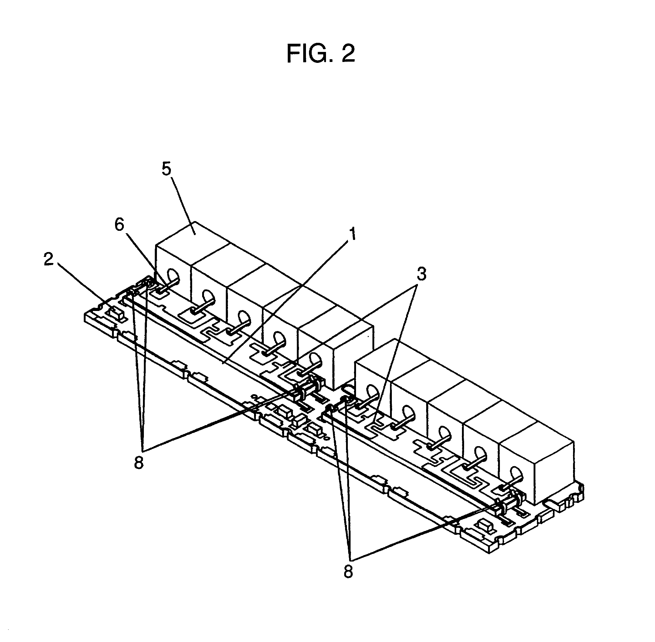
[0001] The present invention relates to a circuit component and a terminal structure thereof, for use in a wireless communication equipment and the like communication apparatus.DESCRIPTION OF THE PRIOR ART[0002] A conventional circuit component and its terminal structure is described in the following using a dielectric filter as an example. FIG. 22 and FIG. 23 show perspective views of a conventional dielectric filter.[0003] Referring to FIG. 23 and FIG. 24, a conventional dielectric filter comprises a coupling board 3 having electrodes formed thereon, a plurality of resonators 5, center conductors 6 and shield covers 7. A circuit board 1 is provided with a grounding pattern and other electrode patterns, which are not shown in the drawing. Also, chip components 2 are mounted on the circuit board 1.[0004] The coupling board 3 is mounted on the circuit board 1 via a spacer 4. The coupling board 3 is provided on the upper and the bottom surfaces with independent electrodes.[0005] A gen...

Claims


Application Information

Patent Timeline
Patent Type & Authority Applications(United States)
IPC IPC(8): H01P1/00H01P1/202H01P1/205H05K1/11H05K1/14H05K3/34H05K3/36
CPCH01P1/00H01P1/2053H01R12/57H05K3/3405H05K3/3426H05K3/368H05K2201/10386H05K2201/10757H05K2201/10772H01R12/52H01R12/718H01R12/721Y02P70/50
Inventor NARUSE, TAKUMIKOZAKI, KENICHIEGUCHI, KAZUHIROSASAKI, KATSUMI
Owner PANASONIC CORP
Learn More