Semiconductor device

a technology of semiconductors and devices, applied in the direction of semiconductor devices, basic electric elements, electrical equipment, etc., can solve the problems of high breakdown voltage etc., and achieve the effect of low on-resistance, high switching speed, and high switching speed

Active Publication Date: 2022-11-01
POWER MASTER SEMICON CO LTD
View PDF18 Cites 0 Cited by
  • Summary
  • Abstract
  • Description
  • Claims
  • Application Information

AI Technical Summary

Benefits of technology

[0007]The present disclosure has been made in an effort to provide a super-junction semiconductor device having excellent reliability and stability while down-sizing a chip.
[0027]According to the exemplary embodiments of the present disclosure, an upper portion with reference to the center of the active region ACT pillar is P-rich and a lower portion is N-rich while the P-type charge amount and the N-type charge amount are balanced near the center of the active region ACT pillar in the vertical direction, and the charge amount is gradually increased in the upper portions of the P pillar and the N pillar in the vertical direction and the charge amount is gradually decreased in the lower portions of the P pillar and the N pillar such that, during a turn-off switching operation, an increasing speed of a width of a depletion layer in the upper region of the N pillar according to an increase of a drain voltage is set to be slowed down, to thereby accelerate formation of a charge pocket and increase a parasitic capacitance value CGD due to the charge pocket.
[0028]Accordingly, the drain voltage VDS can be prevented from being rapidly changed due to the effect of increasing the parasitic capacitance value CGD while down-sizing the chip, and thus the EMI characteristic, overshoot of the drain voltage VDS, and oscillation or spiking of the gate voltage VGS can be remarkably improved. In addition, the semiconductor device according to the exemplary embodiments of the present disclosure has a unique symmetry that increases the amount of charge in both the P pillar and the N pillar toward the top of the active area (ACT), and decreases the amount of charge in both the P pillar and the N pillar toward the bottom, and thus it is possible to minimize negative effects such as a decrease in BVDSS or a change in the resistance value RDS(ON) of an element device according to the charge amount imbalance. Accordingly, the semiconductor device according to the exemplary embodiments of the present disclosure can secure reliability and stability while realizing down-sizing of the chip.

Problems solved by technology

A power-type metal oxide semiconductor field effect transistor (MOSFET) may be used as a switch, and requires low on-resistance, a high breakdown voltage, and high switching speed.
In such a case, the switching speed increases because down-sizing of the chip reduces the capacitance between the gate and drain in the super-junction MOSFET, but at the same time, electromagnetic interference (EMI) problems, problems of increasing voltage overshoot, problems of increasing gate voltage oscillation or spiking, and the like may occur.

Method used


Image

  • Semiconductor device
  • Semiconductor device
  • Semiconductor device

Examples


Embodiment Construction

[0039]The present disclosure will be described more fully hereinafter with reference to the accompanying drawings, in which exemplary embodiments of the disclosure are shown. As those skilled in the art would realize, the described embodiments may be modified in various different ways, all without departing from the spirit or scope of the present disclosure. Accordingly, the drawings and description are to be regarded as illustrative in nature and not restrictive. Like reference numerals designate like elements throughout the specification.

[0040]In addition, unless explicitly described to the contrary, the word “comprise” and variations such as “comprises” or “comprising” will be understood to imply the inclusion of stated elements but not the exclusion of any other elements.

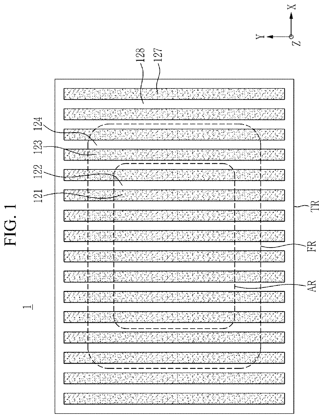
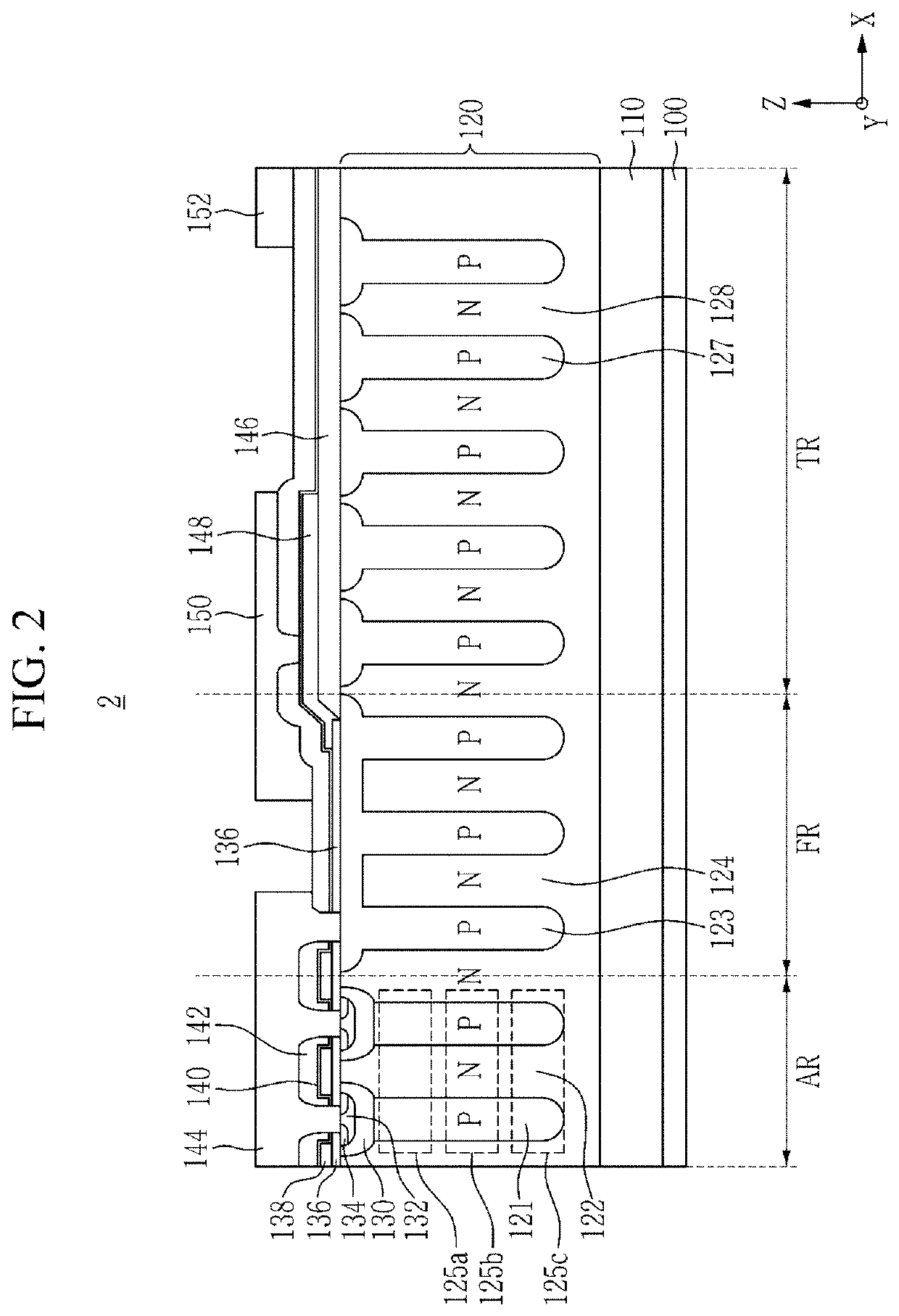
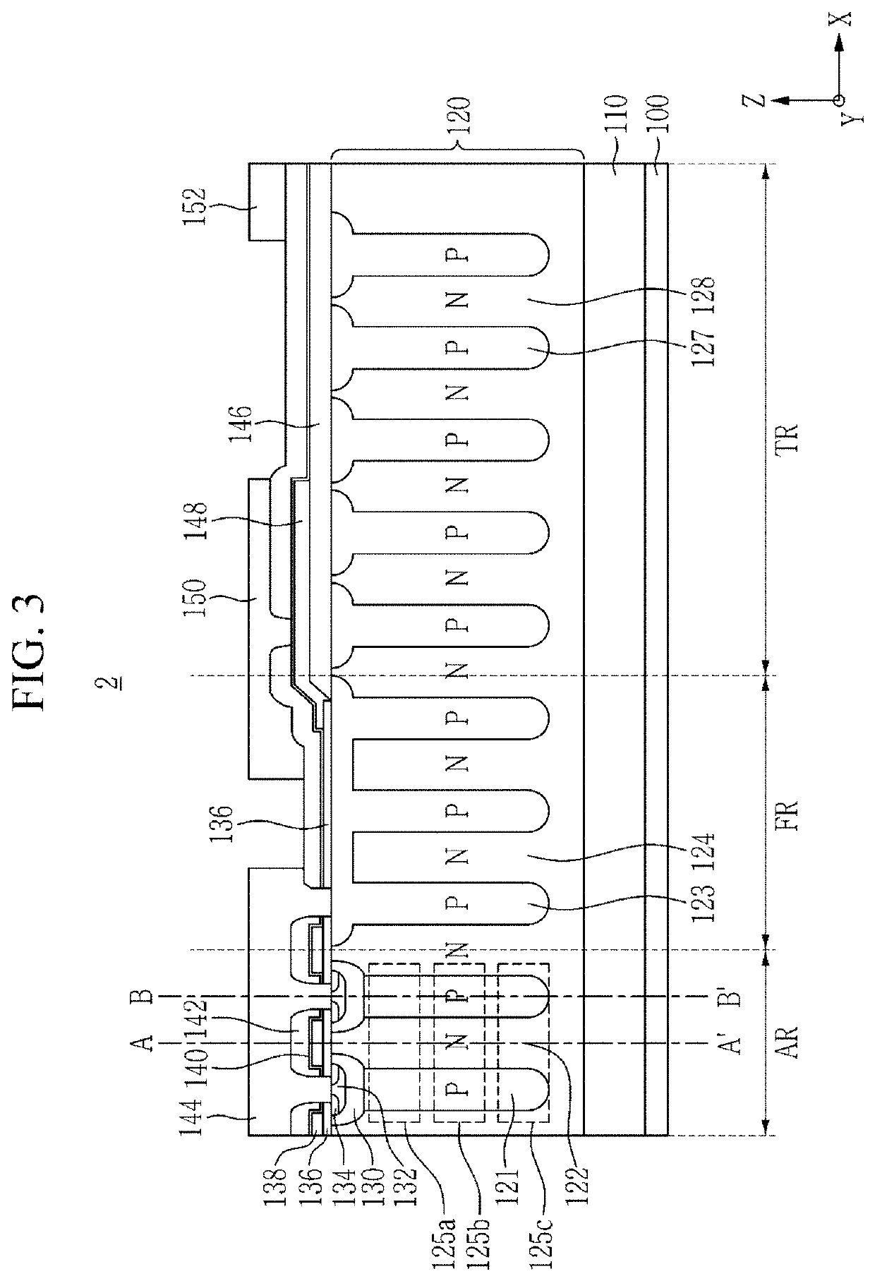
[0041]Although exemplary embodiments of the present disclosure are mainly described with an example of a super-junction semiconductor device, the technical spirit of the present disclosure is not limited thereto...


PUM

PropertyMeasurementUnit
chargeaaaaaaaaaa
P-type chargeaaaaaaaaaa
drain voltageaaaaaaaaaa

Abstract

A semiconductor device is provided. A semiconductor device includes: a first semiconductor layer having an N-type conductivity; and a second semiconductor layer that is formed on the first semiconductor layer, wherein an active region is defined in the first semiconductor layer and the second semiconductor layer, the active region includes a plurality of first P pillars and a plurality of first N pillars alternately arranged along a first direction, in the active region, an upper pillar region including an upper region of the plurality of first P pillars and an upper region of the plurality of first N pillars, a lower pillar region including a lower region of the plurality of first P pillars and a lower region of the plurality of first N pillars, and a middle pillar region formed between the upper pillar region and the lower pillar region are defined, the entire charge amount of the upper pillar region is greater than the entire charge amount of the lower pillar region, and a P-type charge amount is greater than an N-type charge amount in the upper pillar region, while the N-type charge amount is greater than the P-charge amount in the lower pillar region.

Description

CROSS-REFERENCE TO RELATED APPLICATION[0001]This application claims priority to and the benefit of Korean Patent Application No. 10-2020-0033888 filed in the Korean Intellectual Property Office on Mar. 19, 2020, the entire contents of which are incorporated herein by reference.BACKGROUND(a) Technical Field[0002]The present disclosure relates to a semiconductor device.(b) Description of the Related Art[0003]A power-type metal oxide semiconductor field effect transistor (MOSFET) may be used as a switch, and requires low on-resistance, a high breakdown voltage, and high switching speed. In particular, a super-junction MOSFET, which is a representative example of a high breakdown voltage MOSFET, is a kind of Si-MOSFET, and has a high speed switching operation at relatively low power compared to an insulated gate bipolar transistor (IGBT).[0004]By improving the fact that when the breakdown voltage is increased, a drift layer is thickened and thus on-resistance is increased in a planar MO...

Claims


Application Information

Patent Timeline
Patent Type & Authority Patents(United States)
IPC IPC(8): H01L29/06H01L29/78H01L29/66H01L21/266H01L21/225H01L21/265
CPCH01L29/0634H01L21/2253H01L21/266H01L21/26513H01L29/66712H01L29/7811H01L29/1095H01L29/402
Inventor LEE, JAEGILHAN, SANGTAE
Owner POWER MASTER SEMICON CO LTD
Why Eureka
Try Eureka