AM-EWOD array element circuitry with high sensitivity for small capacitance

a technology of array element circuitry and capacitance, applied in the field of droplet microfluidic devices, can solve the problems of insufficient capacitance sensitivity of conventional array element circuits, inability to analyze, and inability to achieve large changes in output signals, etc., to achieve the effect of facilitating electronic height measuremen

Active Publication Date: 2021-05-04
SHARP LIFE SCI EU LTD
View PDF10 Cites 0 Cited by
  • Summary
  • Abstract
  • Description
  • Claims
  • Application Information

AI Technical Summary

Benefits of technology

[0028]A more sensitive impedance sensing circuit would allow a more reliable detection of oil filling and air bubbles, as well as other conditions that are associated with small capacitance variations, based on the output from the sensor readout transistor. For example, this further could enable detection of contamination on the device surface and potentially facilitate electronic measurement of the height of the cell gap in which the droplets are located, and be applicable to other device and droplet conditions as well.
[0029]The present invention, therefore, pertains to enhanced configurations of array element circuitry in AM-EWOD devices, which realize improved sensitivity of the impedance sensing circuitry within the array elements. The sensing circuitry is improved by enhancing the sensitivity to very small capacitance variations, such as for example capacitances associated with oil filling and the presence of air bubbles, or as may be suitable to perform electronic measurement of the height of the cell gap between the lower and upper substrates, and other applications. In the array element circuitry in accordance with embodiments of the present invention, small changes of capacitance can be transduced into a higher amplified output current from the sensor readout transistor to permit improved sensing of conditions that are associated with small capacitance variations.
[0030]To accomplish such enhanced sensitivity, a pre-charging effect is applied whereby the sensor readout transistor in an array element being sensed is altered to turn on the sensor readout transistor during a sensing phase. This differs from conventional configurations in which the sensor readout transistor is reset to an off state at the beginning of the sensing phase prior to applying the perturbation voltage. For example, a positive pre-charging voltage may be applied across the gate and source of the sensor readout transistor to turn said transistor on, or a negative voltage may be applied across the gate and source of a p-type sensor readout transistor to turn on the sensor readout transistor.

Problems solved by technology

Even with the advantages of TFT based AM-EWOD devices, analytical challenges remain.
In particular, conventional configurations of array element circuits lack sufficient sensitivity to small capacitances for sensing under certain circumstances.
This results in large part from the gate of the sensor readout transistor initially being at a low voltage, resulting in the sensor readout transistor being in the “off” state, during the reset operation.
Accordingly, small capacitance variations that occur during the sensing operation do not result in a sufficiently large change to the output signal as any small changes to the gate voltage of T3 will not take the transistor out of the “off” state.
Circumstances such as oil filling and the presence of air bubbles result in signal output current swings from the sensor readout transistor comparable to the system noise (of the order of about 20 mV of the final device output voltage), and thus such an output signal is difficult to detect for sensing purposes.

Method used


Image

  • AM-EWOD array element circuitry with high sensitivity for small capacitance
  • AM-EWOD array element circuitry with high sensitivity for small capacitance
  • AM-EWOD array element circuitry with high sensitivity for small capacitance

Examples


Embodiment Construction

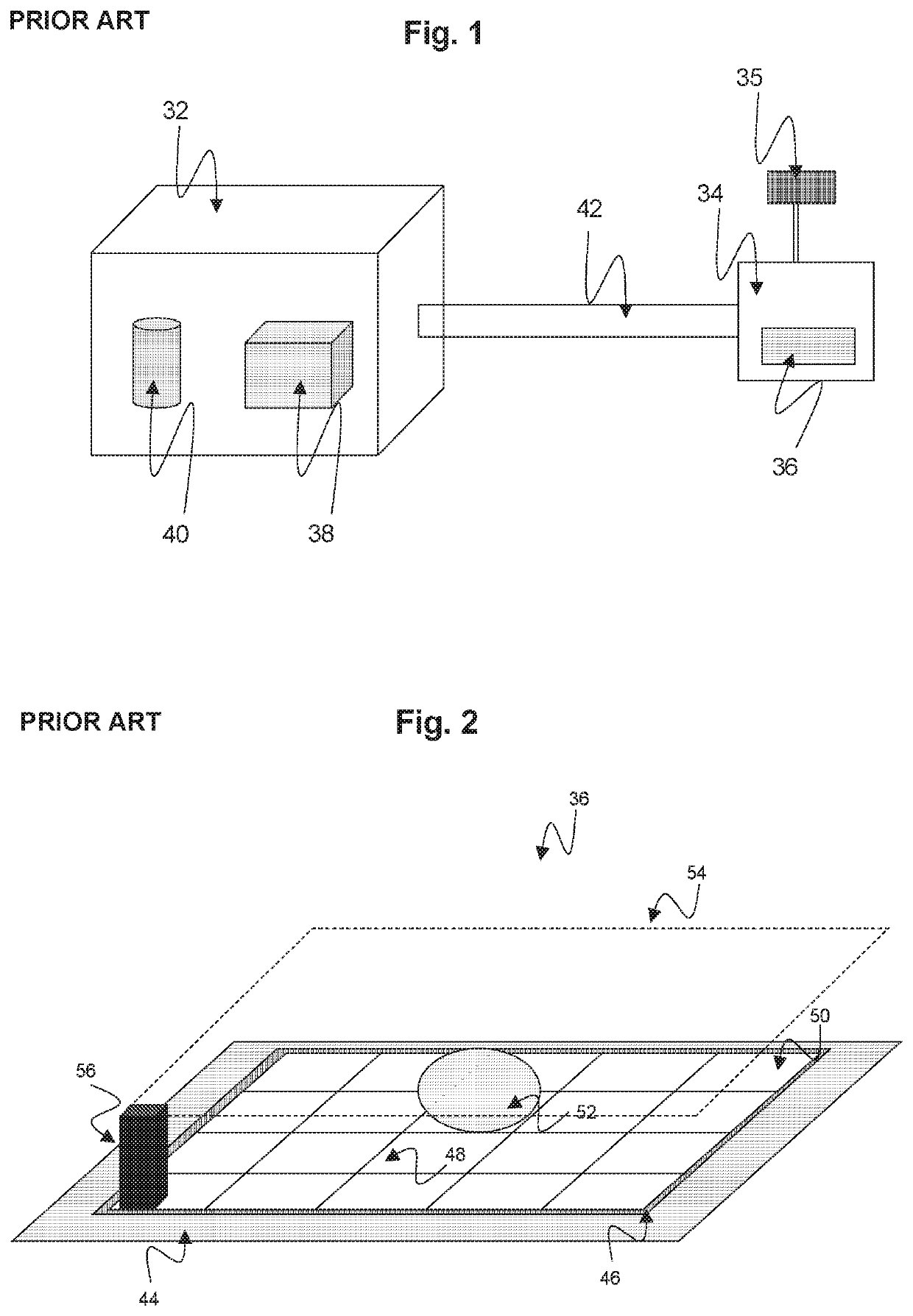
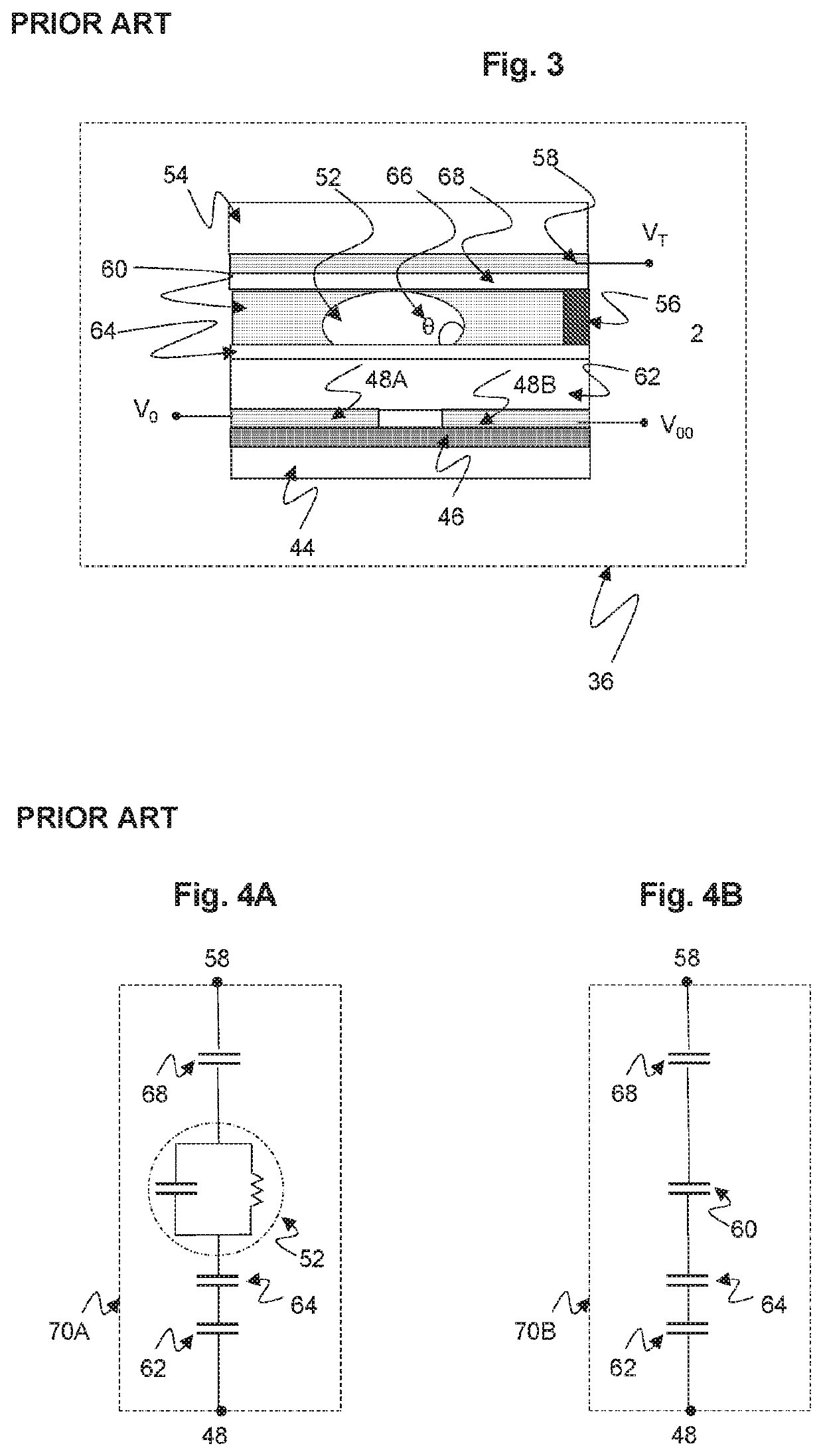
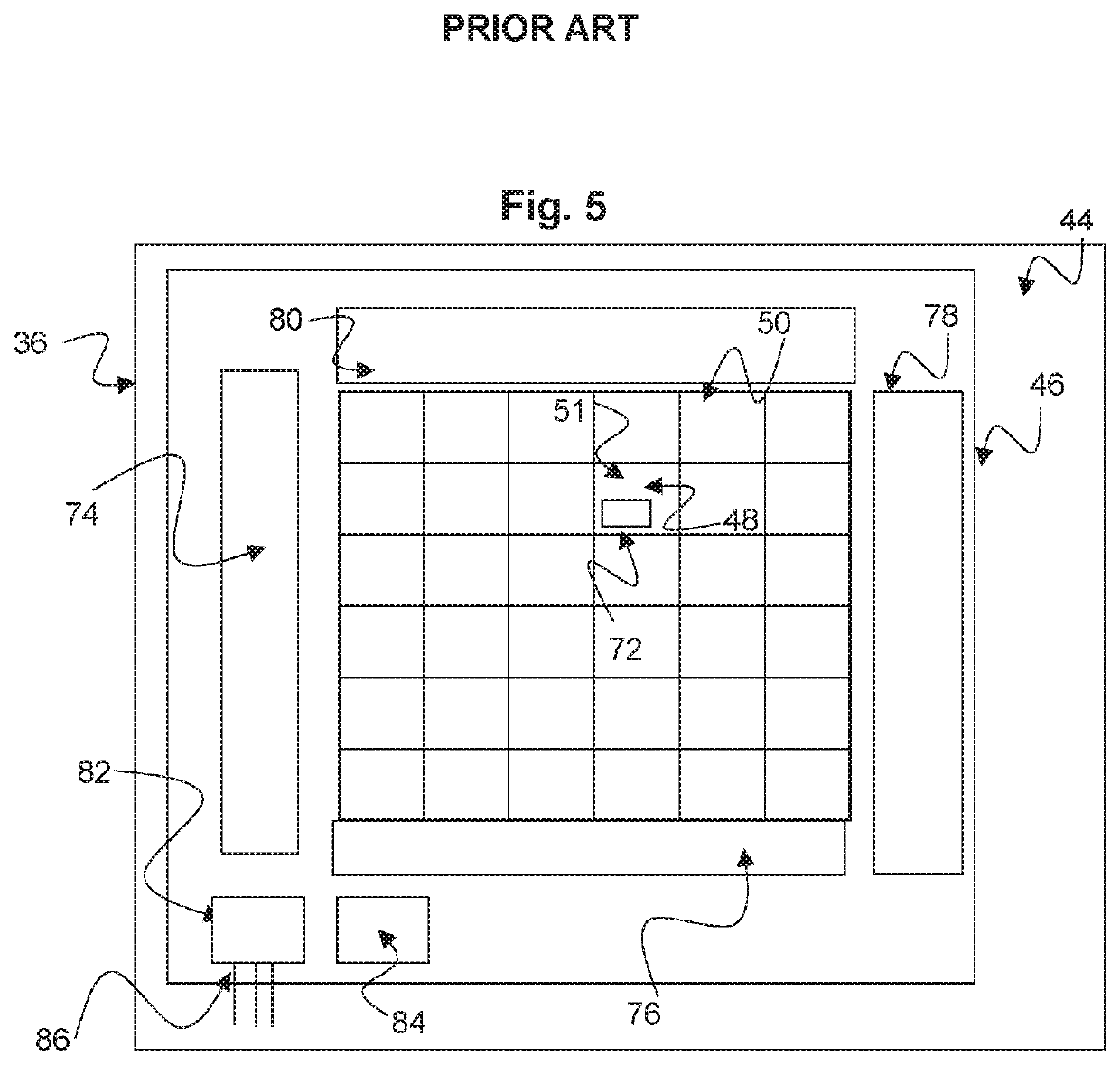
[0067]Embodiments of the present invention will now be described with reference to the drawings, wherein like reference numerals are used to refer to like elements throughout. It will be understood that the figures are not necessarily to scale.

[0068]The present invention pertains to enhanced configurations of array element circuitry in AM-EWOD devices, which realize improved sensitivity of the impedance sensing circuitry within the array elements. The sensing circuitry is improved by enhancing the sensitivity to small capacitance changes, such as for example capacitances associated with oil filling and the presence of air bubbles, or as may be suitable to perform electronic measurement of the height of the cell gap in which the droplets may be received, and other applications. In the array element circuitry in accordance with embodiments of the present invention, small changes of capacitance can be transduced into a higher amplified output current from the sensor readout transistor....


PUM


Abstract

An AM-EWOD device includes a plurality of array elements arranged in an array of rows and columns, each of the array elements including array element circuitry, an element electrode, and a reference electrode. The array element circuitry includes actuation circuitry configured to apply actuation voltages to the element and / or reference electrodes for actuating the array element, and impedance sensor circuitry configured to sense impedance at the array element electrode to determine a droplet or device property at the array element, the impedance sensor circuitry comprising a sensor capacitor and a sensor readout transistor that outputs an output current for sensing. The sensor capacitor is electrically connected to a gate of the sensor readout transistor such that during a sensing phase a voltage perturbation is coupled through the sensor capacitor (and possibly other circuit elements) to the gate of the sensor readout transistor. The impedance sensor circuitry further comprises a pre-charging element that operates to turn on the sensor readout transistor during the sensing phase in combination with coupling of the voltage perturbation, thereby increasing the effect of the voltage perturbation on the output current.

Description

TECHNICAL FIELD[0001]The present invention relates to droplet microfluidic devices, and more specifically to Active Matrix Electrowetting-On-Dielectric (AM-EWOD) devices and to configurations of the array element circuitry of the array elements of such a device to optimize sensing capabilities particularly for low capacitance sensing.BACKGROUND ART[0002]Electrowetting on dielectric (EWOD) is a well-known technique for manipulating droplets of fluid by application of an electric field. Active Matrix EWOD (AM-EWOD) refers to implementation of EWOD in an active matrix array incorporating transistors, for example by using thin film transistors (TFTs). It is thus a candidate technology for digital microfluidics for lab-on-a-chip technology. An introduction to the basic principles of the technology can be found in “Digital microfluidics: is a true lab-on-a-chip possible?”, R. B. Fair, Microfluid Nanofluid (2007) 3:245-281).[0003]FIG. 1 is a drawing depicting an exemplary EWOD based microf...

Claims


Application Information

Patent Timeline
Patent Type & Authority Patents(United States)
IPC IPC(8): G09G3/34G02B26/00H01L27/12
CPCG09G3/348G02B26/005H01L27/124H01L27/1255G09G2300/0809G09G2330/12G01N27/028G01N27/226G01N27/228B01L3/5027B01L3/502792B01L2200/0673B01L2200/143B01L2300/0645B01L2400/0427
Inventor BEARD, OLIVER JAMESHADWEN, BENJAMIN JAMES
Owner SHARP LIFE SCI EU LTD
Why Eureka
Try Eureka