Semiconductor device and method of manufacturing same

a semiconductor and semiconductor technology, applied in the direction of semiconductor devices, electrical devices, transistors, etc., can solve the problems of inability to use double diffusion, large number of crystal defects, and low diffusion coefficient of impurity atoms in silicon carbide substrates, so as to suppress the increase of resistance and forward voltage of the body diode and prevent the deviation of mask alignmen

Active Publication Date: 2020-11-17
FUJI ELECTRIC CO LTD
View PDF5 Cites 0 Cited by
  • Summary
  • Abstract
  • Description
  • Claims
  • Application Information

AI Technical Summary

Benefits of technology

[0005]In view of the aforementioned problems, the present invention aims at providing a semiconductor device and a method of manufacturing the same that can prevent mask alignment deviations and can suppress an increase in ON resistance and forward voltage of a body diode.
[0009]The present invention makes it possible to provide a semiconductor device and a method of manufacturing the same that can prevent mask alignment deviations.

Problems solved by technology

However, the diffusion coefficient of impurity atoms in a silicon carbide (SiC) substrate is extremely low, and it is not possible to use double diffusion.
In this method, high concentration ion implantation induces a large number of crystal defects.
This may cause an increase in contact resistance or ON resistance.
Due to this, contact resistance increases, and this is a cause of an increase in ON resistance, an increase in forward voltage of the body diode, etc.

Method used


Image

  • Semiconductor device and method of manufacturing same
  • Semiconductor device and method of manufacturing same
  • Semiconductor device and method of manufacturing same

Examples


embodiment

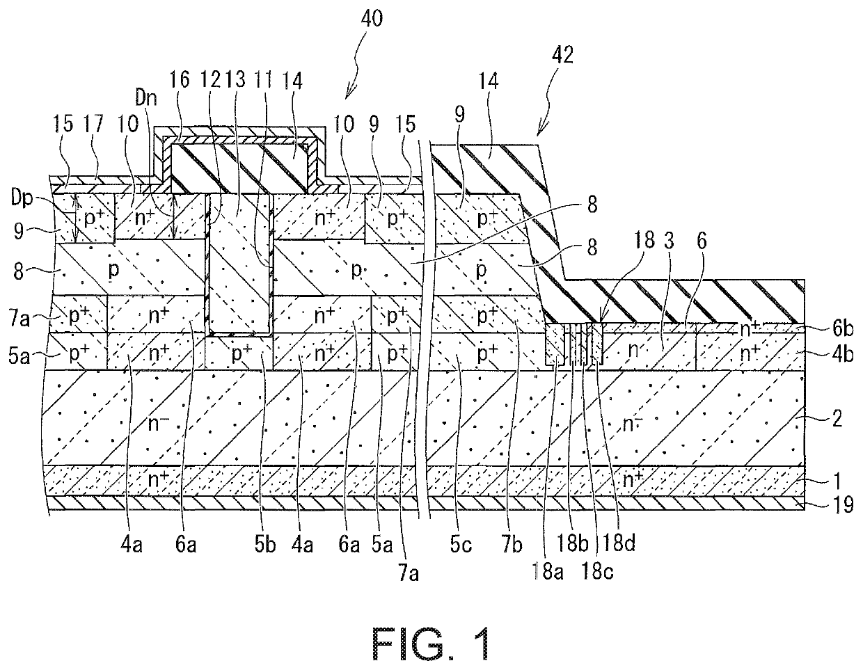
[0031]As shown in FIG. 1, a semiconductor device according to Embodiment 1 of the present invention includes an active region 40, and a mesa structure termination region 42 disposed on the periphery of the active region 40 so as to surround the active region. In FIG. 1, a case is illustratively shown where the active region 40 contains a trench gate structure MOSFET provided as an active element on top of a drift layer 2 of a first conductivity type (n).

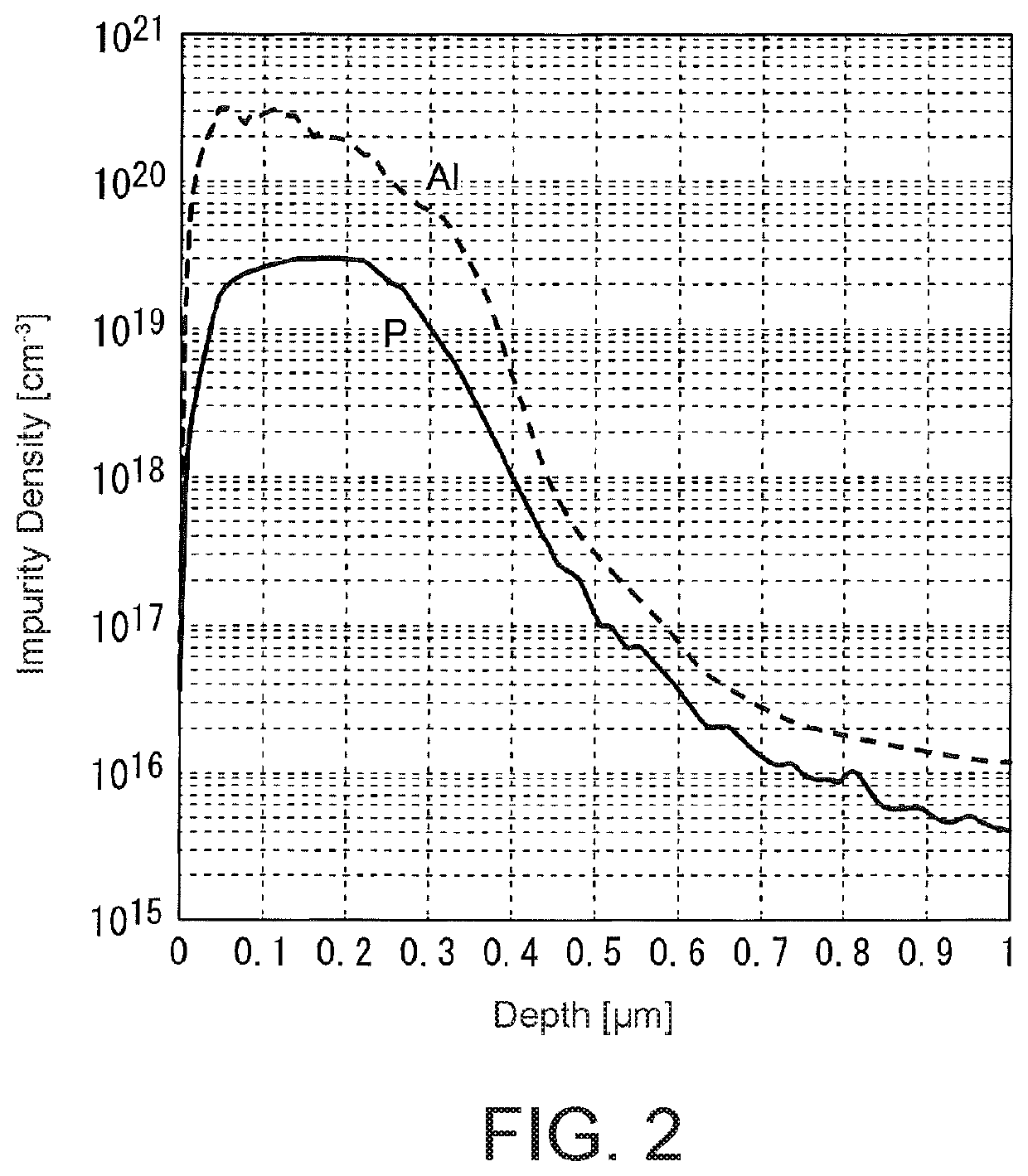
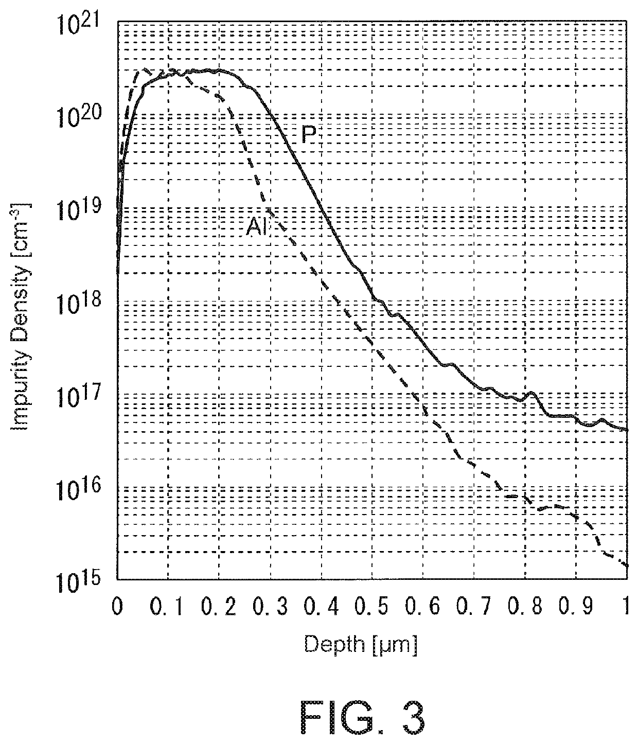
[0032]In the active region 40, an n+ current spreading region (CSL) (4a, 6a) is disposed with a higher impurity density than the drift layer 2 on the top surface of the drift layer 2. A base region 8 of a second conductivity type (p-type) is disposed on the top surface of the current spreading region (4a, 6a). The drift layer 2 and base region 8 are each formed by epitaxially grown layers made of SiC (hereinafter abbreviated as “epitaxial layers”). The current spreading region (4a, 6a) is formed by implantation layers 4a, 6a in which...


PUM

PropertyMeasurementUnit
depth Dnaaaaaaaaaa
depth Dnaaaaaaaaaa
depthaaaaaaaaaa

Abstract

A semiconductor device includes a current spreading region of the first conductivity type provided on a drift layer and having a higher impurity density than the drift layer; a base region of a second conductivity type provided on the current spreading region; a base contact region of the second conductivity type provided in a top part of the base region and having a higher impurity density than the base region; and an electrode contact region of the first conductivity type provided in a top part of the base region that is laterally in contact with the base contact region, the electrode contact region having a higher impurity density than the drift layer, wherein a density of a second conductivity type impurity element in the base contact region is at least two times as much as a density of a first conductivity type impurity element in the electrode contact region.

Description

BACKGROUND OF THE INVENTIONTechnical Field[0001]The present invention relates to a semiconductor device, and particularly relates to a semiconductor device that suppresses an increase in contact resistance and a method of manufacturing the same.Background Art[0002]In a MOS field effect transistor (MOSFET) that uses silicon (Si), double diffusion is used to form, in a p-type well region, an n+ source region to which a high concentration of impurities has been added. However, the diffusion coefficient of impurity atoms in a silicon carbide (SiC) substrate is extremely low, and it is not possible to use double diffusion. To address this, in a MOSFET that uses SiC, double ion implantation is used to form the p-type well region, and the n+ source region in the well region. In this method, high concentration ion implantation induces a large number of crystal defects. This may cause an increase in contact resistance or ON resistance. To solve such a problem, it has been proposed that a p-t...

Claims


Application Information

Patent Timeline
Patent Type & Authority Patents(United States)
IPC IPC(8): H01L29/78H01L29/36H01L29/10H01L29/423H01L29/08H01L21/04H01L29/66H01L29/16
CPCH01L29/0865H01L29/086H01L29/7811H01L29/7813H01L29/1608H01L21/046H01L29/4236H01L29/1095H01L29/66068H01L29/36H01L29/0661H01L29/0878H01L29/0623H01L29/66734H01L29/0619H01L29/0638H01L29/7397
Inventor OKUMURA, KEIJI
Owner FUJI ELECTRIC CO LTD
Why Eureka
Try Eureka