Semiconductor light emitting diode

a light-emitting diode and semiconductor technology, applied in the direction of basic electric elements, electrical appliances, semiconductor devices, etc., can solve the problems of emerging major problems such as luminous efficiency, and achieve the maximum luminous efficiency excellent light-emitting characteristics of the semiconductor light-emitting diode, and increase conductivity

Active Publication Date: 2019-08-27
LUMENS
View PDF26 Cites 0 Cited by
  • Summary
  • Abstract
  • Description
  • Claims
  • Application Information

AI Technical Summary

Benefits of technology

[0026]In the embodiments of the semiconductor light emitting diode according to the present invention, the interconnection electrodes filled in the via-holes and the ohmic contact layers formed between the interconnection electrodes and the transparent electrode ensure increased conductivity, achieving maximum luminous efficiency of the semiconductor light emitting diode.
[0027]In addition, the formation of the non-conductive reflection film with high reflectance for light in the UV region contributes to excellent light output characteristics of the semiconductor light emitting diode. Excellent light output characteristics of the semiconductor light emitting diode can be obtained also when a lead frame plated with copper or gold is provided.
[0028]Furthermore, ohmic contacts are formed between the transparent electrode composed of a conductive oxide and the interconnection electrodes composed of a metal material and defects are minimized during fabrication of the semiconductor light emitting diode, achieving good bonding between the transparent electrode and the interconnection electrodes.

Problems solved by technology

With the recent increasing demand for highly efficient LEDs, an improvement in luminous efficiency is emerging as a major issue.

Method used


Image

  • Semiconductor light emitting diode
  • Semiconductor light emitting diode
  • Semiconductor light emitting diode

Examples


first embodiment

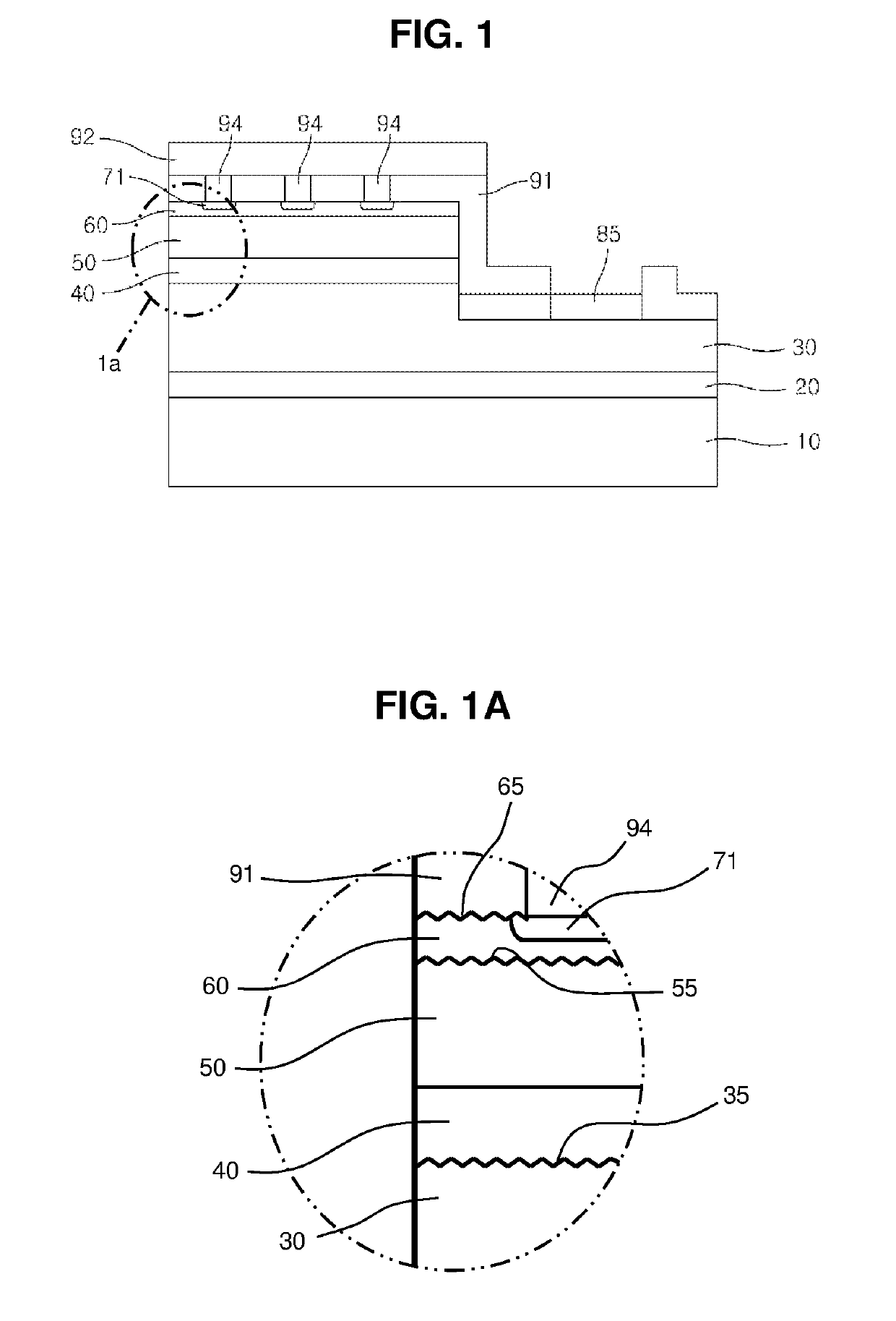
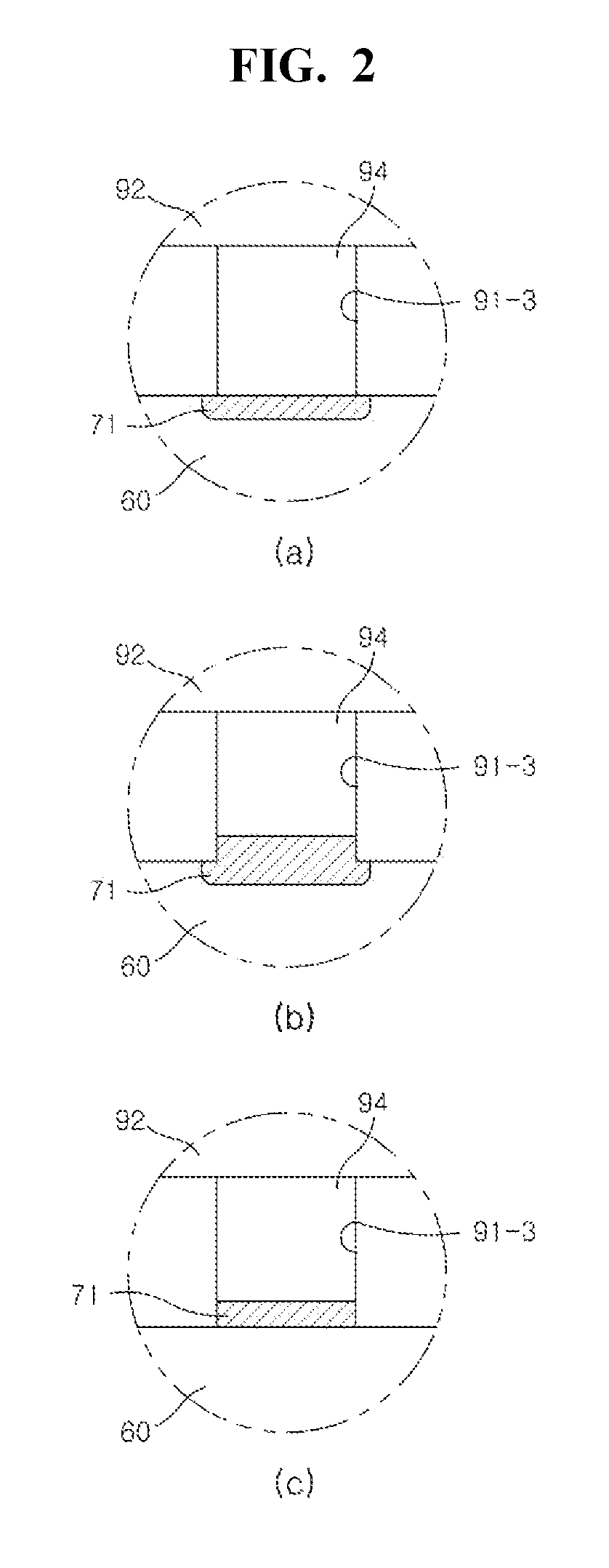
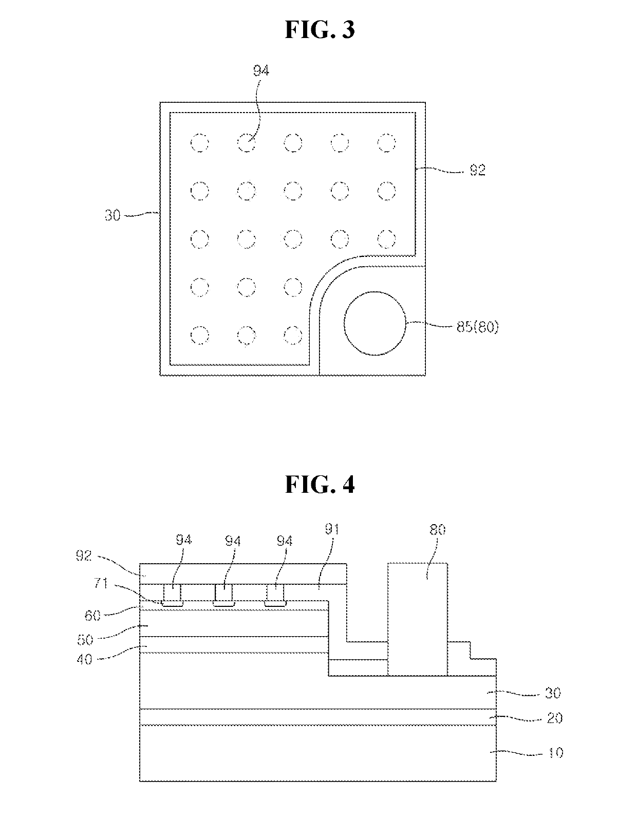
[0041]FIG. 1 is a cross-sectional view of a semiconductor light emitting diode according to the present invention and FIG. 2 illustrates enlarged cross-sectional views for explaining structures in which interconnection electrodes 94 are connected to a transparent electrode 60 in FIG. 1.

[0042]As illustrated in FIGS. 1 and 2, the first embodiment of the semiconductor light emitting diode according to the present invention may include a substrate 10, a buffer layer 20, an n-type semiconductor layer as a first conductive semiconductor layer 30, an active layer 40, a p-type semiconductor layer as a second conductive semiconductor layer 50, a transparent electrode 60, ohmic contact layers 71, an n-type bonding pad 85, a non-conductive reflection film 91 having via-holes 91-3, and a reflective electrode 92.

[0043]The substrate 10 is usually composed of sapphire (Al2O3), SiC, Si, GaN or glass. When the light emitting diode is of a flip type, the substrate 10 may be removed from the final str...

fourth embodiment

[0068]Referring to FIG. 6, a description will be given concerning the semiconductor light emitting diode according to the present invention.

[0069]FIG. 6 is a cross-sectional view of a fourth embodiment of the semiconductor light emitting diode according to the present invention. Unlike the first embodiment, the fourth embodiment further includes connection electrodes 70. As illustrated in FIG. 6, each of the connection electrodes 70 may include the ohmic contact layer 71. Alternatively, each of the connection electrodes 70 may be the ohmic contact layer 71. In the fourth embodiment, the transparent electrode 60 and the connection electrodes 70 are sequentially formed and the uppermost layers of the connection electrodes 70 form the ohmic contact layers 71, which are in direct contact with the interconnection electrodes 94.

fifth embodiment

[0070]Referring to FIGS. 7 and 8, a description will be given concerning the semiconductor light emitting diode according to the present invention.

[0071]Specifically, FIGS. 7 and 8 are cross-sectional and plan views of a fifth embodiment of the semiconductor light emitting diode according to the present invention, respectively.

[0072]The same reference numerals are given to the same elements in the fifth embodiment as those in the first to fourth embodiments, and thus a description thereof is omitted.

[0073]The fifth embodiment is distinguished from the first to fourth embodiments in that n-type electrodes 82 are engaged with the interconnection electrodes 94. For this arrangement, the semiconductor light emitting diode of the present invention includes an n-type electrode unit, as illustrated in FIG. 7. The n-type electrode unit 80 may be formed on the first conductive semiconductor layer 30 after removal of portions of the active layer 40, the second conductive semiconductor layer 5...


PUM


Abstract

A semiconductor light emitting diode is disclosed. The semiconductor light emitting diode includes a first conductive semiconductor layer, a second conductive semiconductor layer, an active layer disposed between the first conductive semiconductor layer and the second conductive semiconductor layer, a transparent electrode formed on the second conductive semiconductor layer, a non-conductive reflection film covering the circumferential surface of the transparent electrode and having one or more via-holes formed therein, a reflective electrode formed on the non-conductive reflection film, interconnection electrodes filled in the via-holes and electrically connecting the reflective electrode to the transparent electrode, and ohmic contact layers formed between the transparent electrode and the interconnection electrodes and filled in recesses formed at positions of the transparent electrode corresponding to the via-holes by etching or extending through the via-holes from the recesses.

Description

TECHNICAL FIELD[0001]The present invention is related to a semiconductor light emitting diode with reduced electrical contact resistance and improved luminous efficiency.BACKGROUND ART[0002]A light emitting diode is a device that converts electrical energy into light energy. When a forward voltage is applied to a light emitting diode including an n-type semiconductor layer and a p-type semiconductor layer, electrons from the n-type semiconductor layer combine with holes from the p-type semiconductor layer, and as a result, energy corresponding to the band gap energy between the conduction band and the valence band is usually released in the form of heat or light.[0003]Various types of compound semiconductors are used in the fabrication of light emitting diodes that produce various colors. Particularly, nitride semiconductors are extensively used in the field of photonic device and high power electronic device development due to their good thermal stability and wide band gap energy.[...

Claims


Application Information

Patent Timeline
Patent Type & Authority Patents(United States)
IPC IPC(8): H01L33/38H01L33/62H01L33/46H01L33/42H01L33/40
Inventor YOO, TAE KYUNGKIM, DAE WON
Owner LUMENS
Why Eureka
Try Eureka