Multilayer ceramic electronic component having external electrodes with holes in plating layers
- Summary
- Abstract
- Description
- Claims
- Application Information
AI Technical Summary
Benefits of technology
Problems solved by technology
Method used
Image
Examples
Embodiment Construction
[0019]Hereinafter, exemplary embodiments will now be described in detail with reference to the accompanying drawings.
[0020]Directions of a hexahedron will be defined in order to clearly describe exemplary embodiments in the present disclosure. L, W and T illustrated in the drawings refer to a length direction, a width direction, and a thickness direction, respectively. Here, the thickness direction refers to a stacking direction in which dielectric layers are stacked.
[0021]A multilayer ceramic electronic component according to an exemplary embodiment, particularly a multilayer ceramic capacitor, will hereinafter be described. However, the multilayer ceramic electronic component according to the present disclosure is not limited thereto.
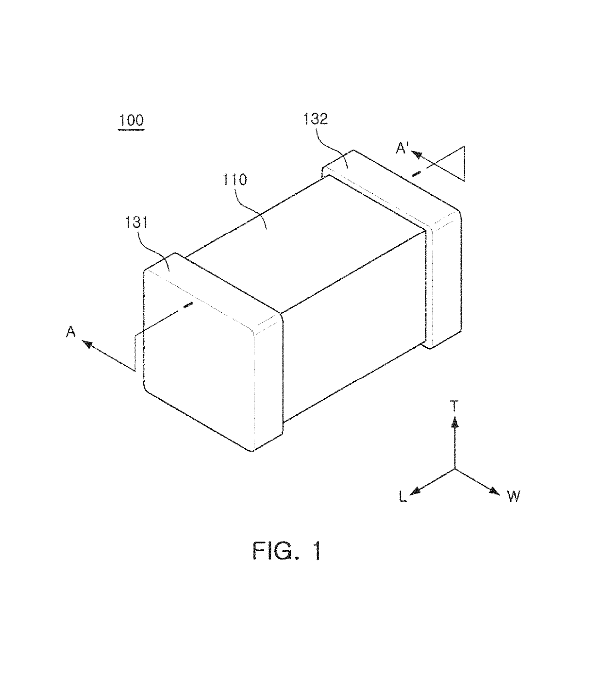
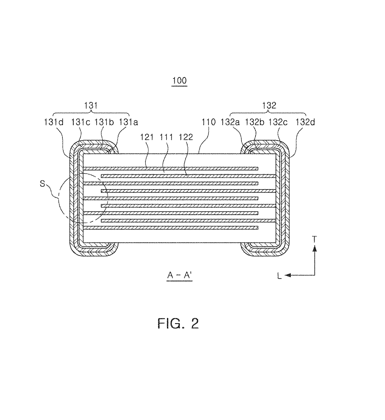
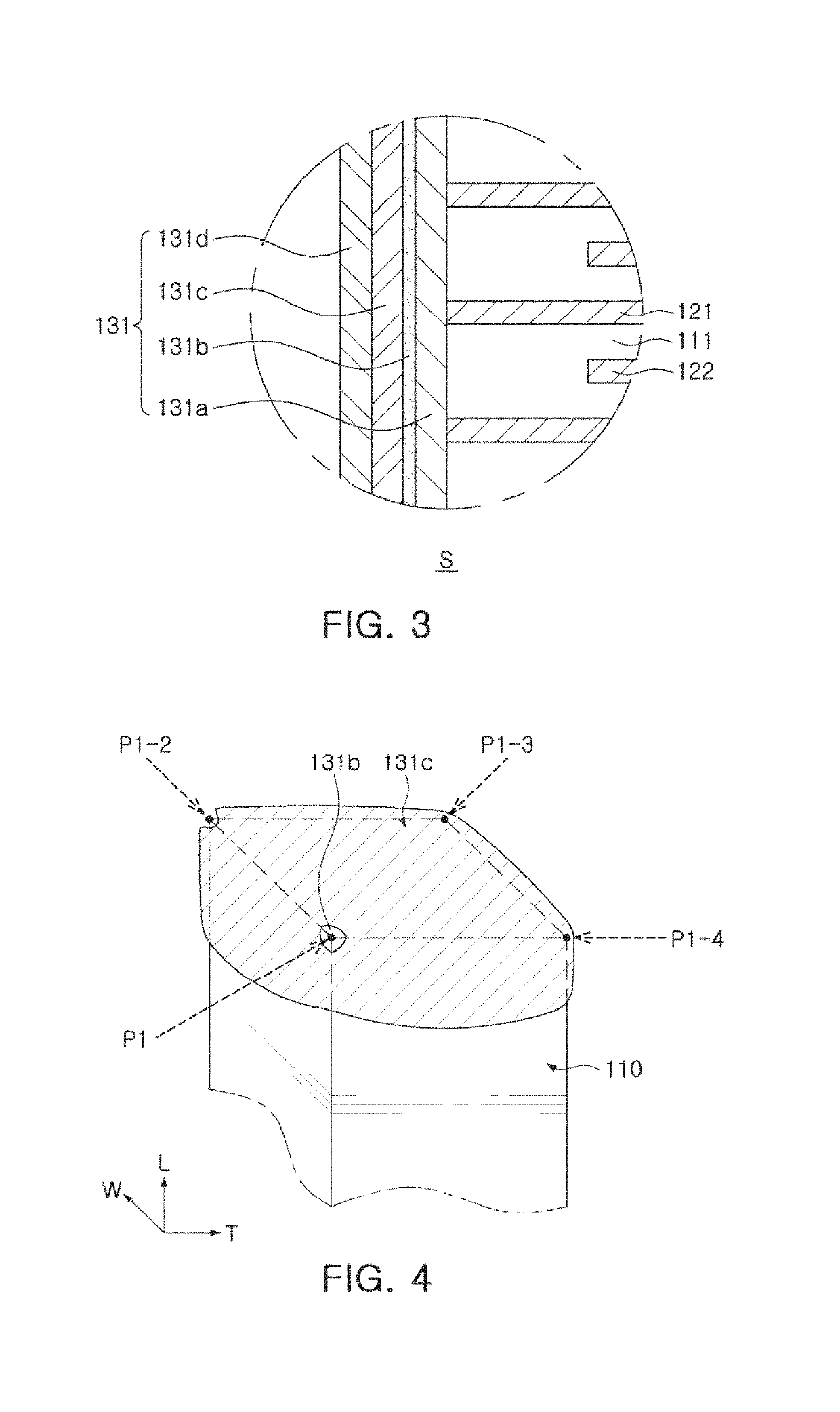
[0022]FIG. 1 is a perspective view illustrating a multilayer ceramic electronic component according to an exemplary embodiment, FIG. 2 is a cross-sectional view taken along line A-A′ of FIG. 1, and FIG. 3 is an enlarged view of region S of FIG. 2.
[002...
PUM
| Property | Measurement | Unit |
|---|---|---|
| Thickness | aaaaa | aaaaa |
| Thickness | aaaaa | aaaaa |
| Thickness | aaaaa | aaaaa |
Abstract
Description
Claims
Application Information
 - R&D
- Intellectual Property
- Life Sciences
- Materials
- Tech Scout
- Unparalleled Data Quality
- Higher Quality Content
- 60% Fewer Hallucinations
Browse by: Latest US Patents, China's latest patents, Technical Efficacy Thesaurus, Application Domain, Technology Topic, Popular Technical Reports.
© 2025 PatSnap. All rights reserved.Legal|Privacy policy|Modern Slavery Act Transparency Statement|Sitemap|About US| Contact US: help@patsnap.com


