Method and apparatus for reducing threshold voltage mismatch in an integrated circuit

a technology of integrated circuits and threshold voltages, applied in the direction of electrical apparatus, basic electric elements, semiconductor devices, etc., can solve the problems of difficult to consistently achieve from device to device, difficult to reduce the number of halo implants, and the difficulty of reducing the number of halo implants, so as to reduce the number of sces and eliminate the need for halo implants

Active Publication Date: 2019-04-30
TAIWAN SEMICON MFG CO LTD
View PDF2 Cites 0 Cited by
  • Summary
  • Abstract
  • Description
  • Claims
  • Application Information

AI Technical Summary

Benefits of technology

[0011]The present invention offers advantages and alternatives over the prior art by providing a transistor on a substrate structure and method of making the same. The transistor includes a work-function metal layer with corner regions that have a work-function tuning species implanted therein via an angled implantation process. The work-function tuning species tune the effective work function of the gate stack to be relatively uniform across the length of the transistor's channel. As a result, Vt of the transistor is more closely controlled, SCEs are minimized and the need for halo implants are eliminated, thus reducing Vtmm between the transistor and other devices associated with the structure.
[0012]Additionally, the transistor includes epitaxially grown source and drain (S / D) regions wherein n-type or p-type dopants are introduced entirely in-situ, thus avoiding any dopant implantation process during epitaxial growth of the S / D regions. As a result, random diffusion of dopant ions into the channel are minimized to further control Vt of the transistor and the need for LDD implants are eliminated, thus further reducing Vtmm between the transistor and other devices associated with the structure.

Problems solved by technology

Therefore Vtmm becomes increasingly problematic for lower scale semiconductor technology class sizes, such as the 14 nanometers (nm) node and beyond.
However, this is hard to consistently achieve from device to device, especially at smaller critical dimensions (CD), wherein most gate stacks will tend to have bottom corner regions that are variously rounded from device to device.
More particularly, this is especially problematic with RMG FETs having titanium nitride (TiN) as a gate work-function metal layer.
With regards to the amount of random diffusion of dopants in a FET's channel, a major contributor to such random diffusion of dopants is the excessive use of annealing processes, such as rapid thermal annealing (RTA), during device formation.
However, each of the above listed features that contribute to increased diffusion of dopants into the channel are utilized to address specific problems or provide specific benefits, during the formation of a FET, making those features difficult to eliminate or replace.
Moreover, annealing is often required to repair damage caused by ion bombardment during dopant implantation, especially in the S / D regions.
Also, Halo implants are used to reduce punch-through leakage current between source and drain, which become increasingly problematic at lower class sizes.

Method used


Image

  • Method and apparatus for reducing threshold voltage mismatch in an integrated circuit
  • Method and apparatus for reducing threshold voltage mismatch in an integrated circuit
  • Method and apparatus for reducing threshold voltage mismatch in an integrated circuit

Examples


Embodiment Construction

[0025]Certain exemplary embodiments will now be described to provide an overall understanding of the principles of the structure, function, manufacture, and use of the methods, systems, and devices disclosed herein. One or more examples of these embodiments are illustrated in the accompanying drawings. Those skilled in the art will understand that the methods, systems, and devices specifically described herein and illustrated in the accompanying drawings are non-limiting exemplary embodiments and that the scope of the present invention is defined solely by the claims. The features illustrated or described in connection with one exemplary embodiment may be combined with the features of other embodiments. Such modifications and variations are intended to be included within the scope of the present invention.

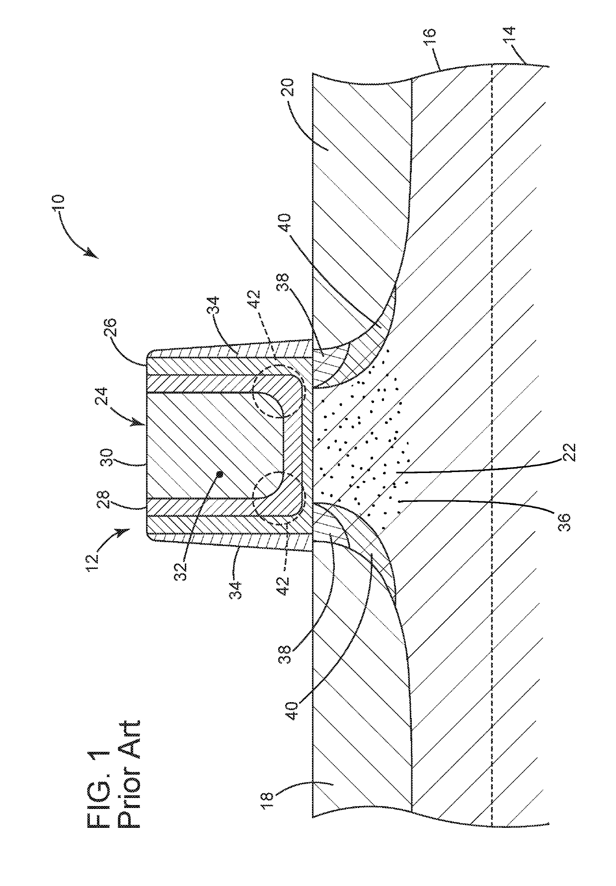
[0026]Referring to FIG. 1, a cross-sectional view of a structure 10 including a prior art planar n-type CMOS FET 12 is presented. Structure 10 includes a substrate 14 into which a ...


PUM


Abstract

A method of making a transistor for an integrated circuit includes providing a substrate and forming a dummy gate for the transistor within a gate trench on the substrate. The gate trench includes sidewalls, a trench bottom, and a trench centerline extending normally from a center portion of the trench bottom. The dummy gate is removed from the gate trench. A gate dielectric layer is disposed within the gate trench. A gate work-function metal layer is disposed over the gate dielectric layer, the work-function metal layer including a pair of corner regions proximate the trench bottom. An angled implantation process is utilized to implant a work-function tuning species into the corner regions at a tilt angle relative to the trench centerline, the tilt angle being greater than zero.

Description

TECHNICAL FIELD[0001]The present invention relates to semiconductor integrated circuits. More specifically, the invention relates to reducing threshold voltage mismatch between field effect transistors of a semiconductor integrated circuit.BACKGROUND[0002]Threshold voltage (Vt) of a field effect transistor (FET) is the minimum gate-to-source voltage differential that is required to create a conducting path through the channel, and between the source and drain (S / D) terminals or regions of the FET. The Vt of devices within a semiconductor integrated circuit is one of the critical parameters that must be carefully controlled and matched from transistor to transistor for proper commercially reproducible operation. This is the case for such FET technologies as planar complementary metal-oxide semiconductor (CMOS) FETs or FinFETs, either of which may be manufactured on bulk semiconductor substrates or silicon-on-insulator (SOI) substrates.[0003]The degree to which Vt will vary between ad...

Claims


Application Information

Patent Timeline
Patent Type & Authority Patents(United States)
IPC IPC(8): H01L21/28H01L29/49H01L29/40H01L21/02H01L29/66H01L29/08
CPCH01L21/28088H01L21/02656H01L21/28114H01L29/66795H01L29/401H01L29/4983H01L29/66545H01L29/0847H01L21/265H01L29/785
Inventor CHI, MIN-HWAZHAO, MEIXIONGKIKUTA, KUNIKO
Owner TAIWAN SEMICON MFG CO LTD
Why Eureka
Try Eureka