Cathodoluminescence-activated nanoscale imaging
a technology of cathodoluminescence and nano-scale, applied in the field of nano-scale imaging, can solve the problems of poor imaging quality, difficult to attach fluorescent labels, damage to soft materials, etc., and achieve the effect of high resolution
- Summary
- Abstract
- Description
- Claims
- Application Information
AI Technical Summary
Benefits of technology
Problems solved by technology
Method used
Image
Examples
example 1
Preparation of an Imaging Chip with a YAlO3:Ce Illumination Layer
[0464]This Example demonstrates the preparation of an imaging chip with a YAlO3 illumination layer containing Ce3+ (YAP:Ce).
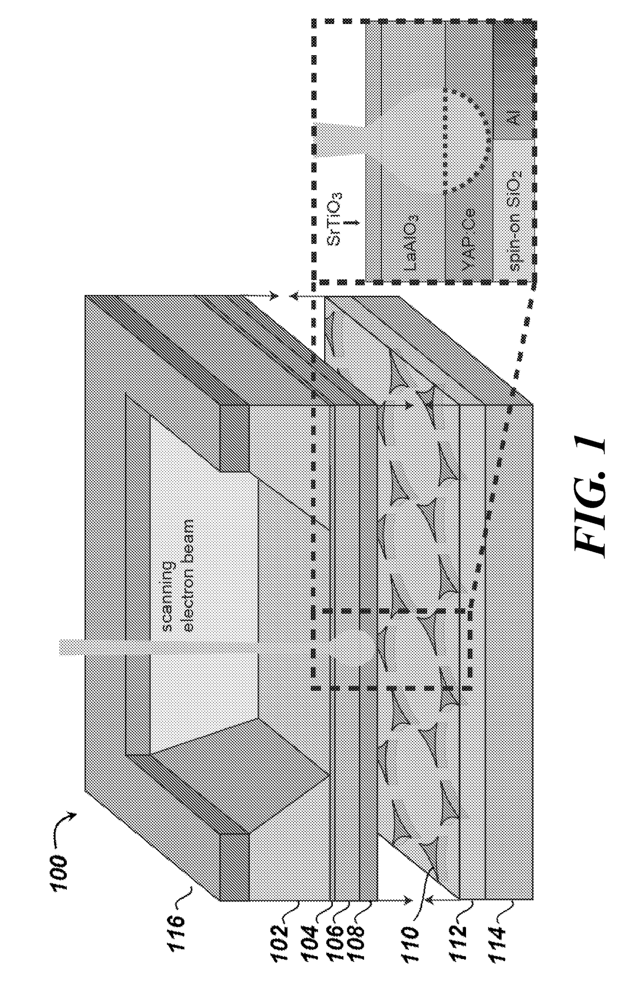
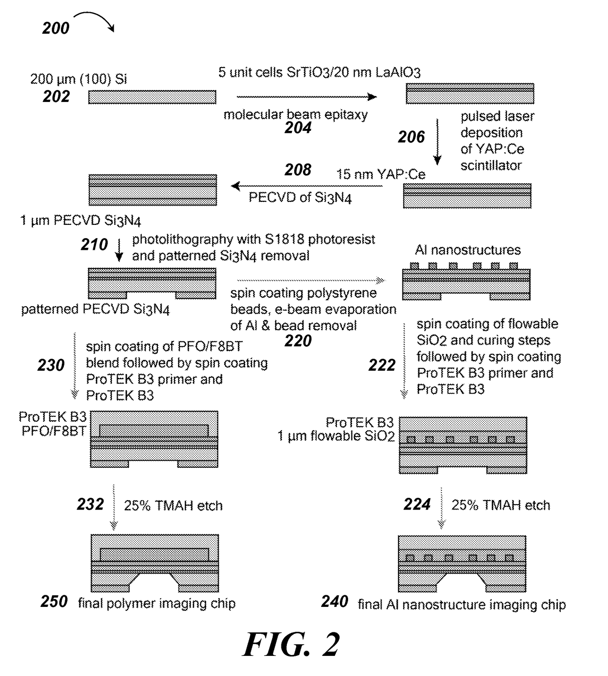
[0465]Onto one side of a 3-inch, 200-μm-thick Si wafer (001) (Virginia Semiconductor) was deposited 5 unit cells of (100)-oriented SrTiO3 followed by 20 nm of (001) LaAlO3 via molecular beam epitaxy (MBE). The (001) and (100) indicate the lattice planes denoted by Miller indices. The wafer was then diced into 5×8 mm chips using a Disco DAD3240 Automatic Dicing Saw in Marvell Nanofabrication Laboratory. Pulsed laser deposition (PLD) was used to deposit 15 nm of YAP:Ce onto the LaAlO3 layer. The PLD source material was a disk of single-crystal YAP:Ce (0.55 wt % Ce, SEMicro), and the laser pulses were generated by a Lambda Physik KrF excimer source operating at a wavelength of 248 nm and pulse-rate of 6 Hz, with a fluence of approximately 0.7 J / cm2. The substrates were held at 750° C. in a 1.0 mTorr ...
example 2
Modification of an Imaging Chip to Include a Sample Layer Containing an Aluminum Nanostructure Sample and Imaging Windows
[0467]This Example demonstrates the addition of an Al nanostructure sample and a sample layer to an imaging chip with a YAP:Ce scintillator film, and the construction of imaging windows in the imaging chip.
[0468]The imaging chip was prepared according to the procedure set forth in Example 1.
[0469]To add the sample to the chip, nanosphere lithography was used to fabricate Al nanostructures on the YAP:Ce film surface of the imaging chip. A 26 mg / ml solution consisting of polystyrene (PS) beads (Bangs Laboratories Inc.) with a 1.0 μm diameter in 8:1 water / methanol with 1% Triton X-100 (Aldrich) were spun onto the YAP:Ce side of the chip. The sequence for the spin coating was 800 rpm / 2000 rpm / s for 10 s, 500 rpm / 2000 rpm / s for 2 min, 2400 rpm / 2000 rpm / s for 20 s, and 6000 rpm / 5000 rpm / s for 6 s. The PS beads formed an incomplete monolayer.
[0470]Using a Semicore SC600 ...
example 3
Modification of an Imaging Chip to Include a Sample Layer Containing an Organic Polymer Sample and Imaging Windows
[0473]This Example demonstrates the addition of a sample of a conjugated polymer blend of polyfluorene (PFO) and poly(9,9-dioctylfluorene-alt-benzothiadiazole) (F8BT) and a sample layer to an imaging chip with a YAP:Ce scintillator film, and the construction of imaging windows in the imaging chip.
[0474]The imaging chip was prepared according to the procedure set forth in Example 1.
[0475]A solution comprising 0.5% PFO (H. W. Sands) and 0.5% F8BT (Solaris Inc.) by weight in o-xylene (Aldrich) was prepared in a glovebox and then filtered through a 0.45 μm syringe filter. The solution was then spun onto the YAP:Ce layer of the imaging chip at 1000 rpm / 2000 rpm / s for 1 minute. Next, polymer was removed with a razor blade from the outer 1 mm of the chip to allow for direct contact between the YAP:Ce chip and the ProTEK® B3 layer and to prevent the PFO / F8BT film from coming int...
PUM
| Property | Measurement | Unit |
|---|---|---|
| thick | aaaaa | aaaaa |
| thick | aaaaa | aaaaa |
| voltage | aaaaa | aaaaa |
Abstract
Description
Claims
Application Information
 - R&D
- Intellectual Property
- Life Sciences
- Materials
- Tech Scout
- Unparalleled Data Quality
- Higher Quality Content
- 60% Fewer Hallucinations
Browse by: Latest US Patents, China's latest patents, Technical Efficacy Thesaurus, Application Domain, Technology Topic, Popular Technical Reports.
© 2025 PatSnap. All rights reserved.Legal|Privacy policy|Modern Slavery Act Transparency Statement|Sitemap|About US| Contact US: help@patsnap.com


