
Link socket sliding mount with preload

a technology of sliding mount and socket, which is applied in the direction of individual semiconductor device testing, coupling device connection, instruments, etc., can solve the problems of high cost and time-consuming maintenance of test equipment, gap between test equipment and socket electrical connector (mount), and high cost of testing equipment. , to achieve the effect of effective connection, quick and reliable testing, and reduced load on test equipmen

Active Publication Date: 2018-10-16
XCERRA
View PDF11 Cites 0 Cited by
  • Summary
  • Abstract
  • Description
  • Claims
  • Application Information

AI Technical Summary

Benefits of technology

The present invention is a test socket with a link and mount system for quickly and reliable testing of microchips after production. The socket includes an elastomer for biasing the link, a pivoting link for connecting to the DUT, and a mount that rotates the link into engagement with the DUT. The mount has projections that extend below the bottom surface of the socket, which ensures successful contact with the test equipment without damaging it. The load on the testing apparatus is dramatically reduced while still maintaining an effective connection between the chip and the apparatus.

Problems solved by technology

While the system of the '669 Patent has been proven effective in the testing of integrated chips, the wear on the test apparatus from the linkage leads to costly and time-consuming maintenance on the test equipment.
The mount in the linkage is rigidly fixed in the test socket, and applies a non-compliant pre-loading on the test apparatus that can lead to excessive wear.
Due to variances between the test equipment and the socket, it is possible that a gap can occur between the test equipment and the socket's electrical connector (mount).
This gap can result in failed tests or improper measurements that can prolong the testing procedure and falsely suggest problems with the DUT.

Method used


Image

  • Link socket sliding mount with preload
  • Link socket sliding mount with preload
  • Link socket sliding mount with preload

Examples


Embodiment Construction

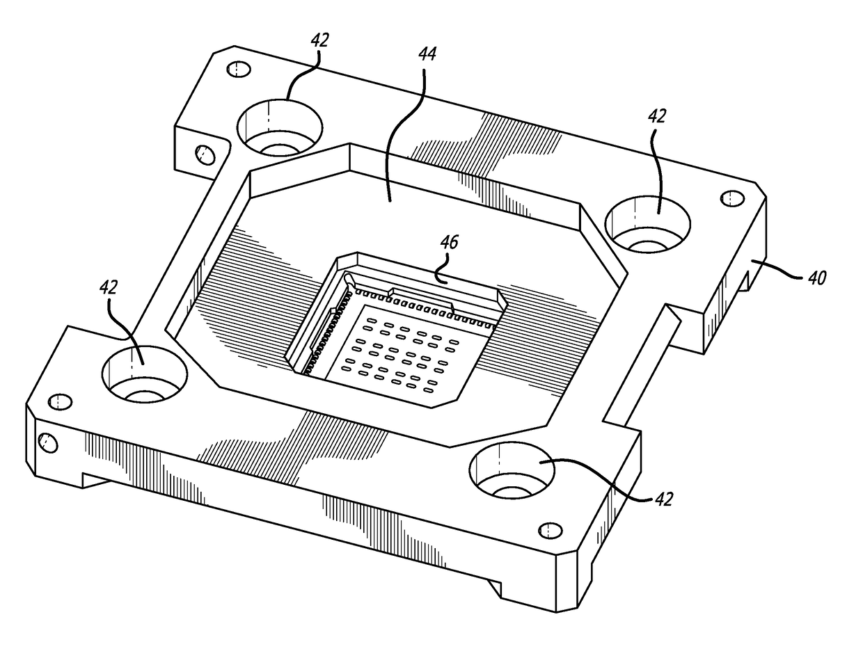
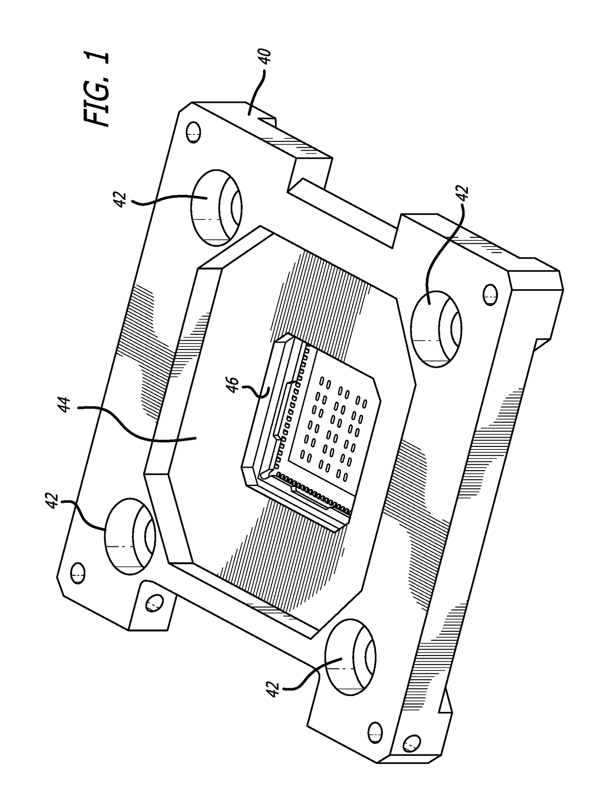
[0015]FIG. 1 illustrates an integrated circuit test socket 40 of the type generally described in U.S. Pat. No. 7,918,669, the contents of which are incorporated herein. The test socket 40 may have a generally square profile with up to four aligning holes 42 to mount the test socket on the testing equipment. On the test socket is a generally square recess 46 is formed to receive the integrated circuit chip under test. A plurality of electrical connections are formed within the recess 46 as described more fully in the '669 patent referenced above. The test socket 40 may be placed, for example, in a handler work press and clamped in the handler in anticipation of testing the integrated chip. Once the socket is mounted in the handler, the chip is inserted into the socket for testing by placing it in the recess 46. Other arrangements, both automated and manual, are also possible with the present invention.

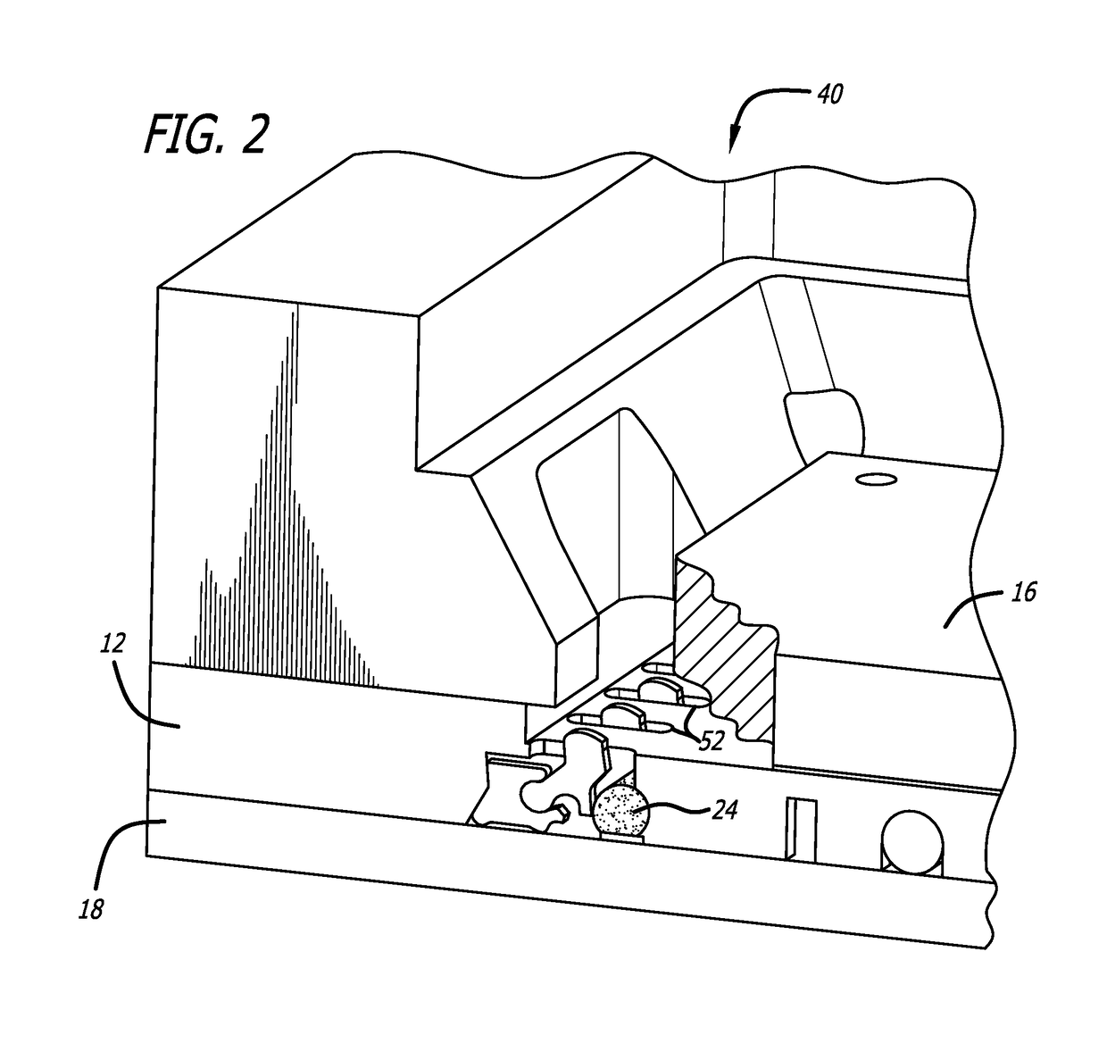
[0016]FIG. 2 illustrates a chip 16 (partially cut away) inserted into the socket 40...


PUM


Abstract

A test socket with a link and mount system is used to couple a device under test to a testing apparatus for quick and reliable testing of microchips post-production. The socket includes a pivoting link that connects to the DUT, an elastomer for biasing the link in a first preferred orientation, and a mount that operates as a fulcrum to rotate the link into engagement with the DUT. The mount includes projections that extend below a bottom surface of the socket, such that engagement of the mount with the test device at the projections translates the mount parallel to a diagonal support wall in the socket such that the mount is driven away from the bottom surface of the socket and also toward the elastomer. The socket includes a gap above the mount to allow for movement of the mount within the socket, eliminating the fixed arrangement and the non-compliant loads that accompany the engagement of the mount to the test apparatus. The mount projections carry a small preload that ensures successful contact with the test equipment without the risk of damaging the test equipment with rigid contact surfaces.

Description

BACKGROUND[0001]Microchips have become prevalent in virtually all types of industries, and the demand for microchips has skyrocketed over the last ten years. This has placed pressure on the industry to make more and better chips as the need for microchips continues to rise. A chip connects to a motherboard or other device via a plurality of pins or terminals, which allows the board to communicate with the chip's logic or memory. An example of such a chip may be a memory card or processor for a computer, each of which may be insertable into a particular slot or socket that makes one or more electrical connections with the chip.[0002]Part of the manufacturing process of the chips is the post-production testing of the quality and performance of the chip. Testing helps to diagnose problems in the manufacturing process, and improve production yields for systems that incorporate the chips. Therefore, sophisticated test systems have been developed to ensure that the circuitry in the chip p...

Claims


Application Information

Patent Timeline
Patent Type & Authority Patents(United States)
IPC IPC(8): G01R1/04G01R31/26H01R12/85H01R9/05
CPCG01R1/0433
Inventor MAGNUSON, AARONYAKUSHEV, SERGEYTREIBERGS, VALTSSIKORSKI, DAN
Owner XCERRA
Learn More