


Quick Research
Generate reliable direction feasibility study reports for your R&D in just a few steps.

Technical Q&A
Discover and master advanced knowledge NOW. Basics, ideas, possibilities, all at once.

Find Solutions
As an expert in R&D theories, this can generate solutions to your technical problems instantly.

Evaluate Feasibility
Analyze your overall solution with one click, know your potential R&D risks in advance.

Monitor Landscape
Get weekly tech updates, stay abreast of the latest tech innovations and key insights.
Silicon electrode plate having excellent durability for plasma etching
A plasma and durability technology, applied in the direction of plasma, circuits, electrical components, etc., can solve the problems of wasteful use method, short time, unavoidable, etc., and achieve the effect of reducing the number of replacements
- Summary
- Abstract
- Description
- Claims
- Application Information
AI Technical Summary
Problems solved by technology
Method used
Image

Examples
Embodiment 1
[0033] Dissolve Si raw material with a purity of 11N, initially dope with B and P, and prepare Si solutions containing B: 1-15ppba and P: 1-10ppba respectively. Using this Si solution, a silicon single crystal having a diameter of 300 mm was produced by the CZ method. This ingot was sliced into wafers with a diamond band saw to a thickness of 8 mm, and then cut to produce a silicon single crystal electrode substrate with a diameter of 290 mm and a thickness of 6 mm.
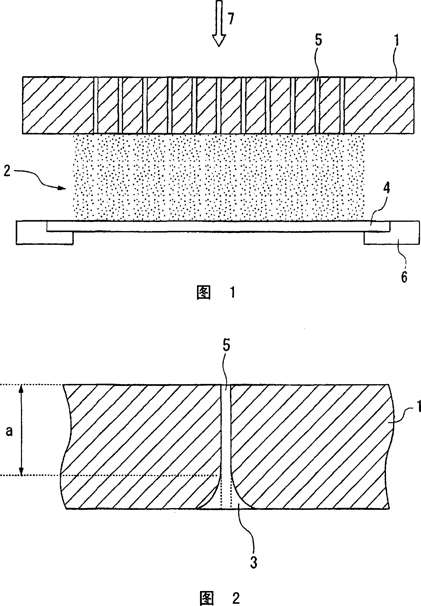
[0034] On this silicon single crystal electrode substrate, penetrating pores with a diameter of 0.3 mm are formed at intervals of 5 mm, and then the surface processing is removed by immersing the silicon single crystal electrode substrate in a mixed solution of hydrofluoric acid, acetic acid, and nitric acid for 5 minutes. Layer, thus made the silicon electrode plate for plasma etching (hereinafter referred to as the electrode plate of the present invention) 1-14 of the present invention having the contents of ...
Embodiment 2
[0047] Dissolve Si raw material with a purity of 11N, initially dope with B and As, and make Si solutions containing B: 1-15ppba and As: 1-10ppba respectively. Using this Si solution, a silicon single crystal having a diameter of 300 mm was produced by the CZ method. This ingot was sliced into wafers with a diamond band saw to a thickness of 8 mm, and then cut to produce a silicon single crystal electrode substrate with a diameter of 290 mm and a thickness of 6 mm.
[0048] On this silicon single crystal electrode substrate, penetrating pores with a diameter of 0.3 mm are formed at intervals of 5 mm, and then the surface processing is removed by immersing the silicon single crystal electrode substrate in a mixed solution of hydrofluoric acid, acetic acid, and nitric acid for 5 minutes. layer, thus making electrode plates 15-28 of the present invention, comparative electrode plates 3, 4 and electrode plate 3 of the prior art.
[0049] The B and As contents of these electrode...
Embodiment 3
[0061] Dissolve Si raw materials with a purity of 11N, initially dope with B, P and As, and make Si solutions containing B: 1-15ppba and P+As: 1-10ppba respectively. Using this Si solution, a silicon single crystal having a diameter of 300 mm was produced by the CZ method. This ingot was sliced into wafers with a diamond band saw to a thickness of 8 mm, and then cut to produce a silicon single crystal electrode substrate with a diameter of 290 mm and a thickness of 6 mm.
[0062] On this silicon single crystal electrode substrate, penetrating pores with a diameter of 0.3 mm are formed at intervals of 5 mm, and then the surface processing is removed by immersing the silicon single crystal electrode substrate in a mixed solution of hydrofluoric acid, acetic acid, and nitric acid for 5 minutes. Layers, electrode plates 29-33 of the present invention and comparative electrode plates 5 and 6 were produced.
[0063] The contents of B, P, and As in these electrode plates were meas...
PUM
| Property | Measurement | Unit |
|---|---|---|
| diameter | aaaaa | aaaaa |
Abstract
Description
Claims
Application Information
 - R&D Engineer
- R&D Manager
- IP Professional
- Industry Leading Data Capabilities
- Powerful AI technology
- Patent DNA Extraction
Browse by: Latest US Patents, China's latest patents, Technical Efficacy Thesaurus, Application Domain, Technology Topic, Popular Technical Reports.
© 2024 PatSnap. All rights reserved.Legal|Privacy policy|Modern Slavery Act Transparency Statement|Sitemap|About US| Contact US: help@patsnap.com