Method for fabricating microlens array with electric controlled and adjusted dimensions
A technology of a microlens array and a manufacturing method, applied in the directions of lenses, optics, instruments, etc., can solve the problems of large volume and inconvenient lens arrays, and achieve the effect of real-time control
- Summary
- Abstract
- Description
- Claims
- Application Information
AI Technical Summary
Problems solved by technology
Method used
Image
Examples
Embodiment Construction
[0017] The present invention will be further described below in conjunction with the embodiments and the accompanying drawings.
[0018] Implementation steps of the present invention are:
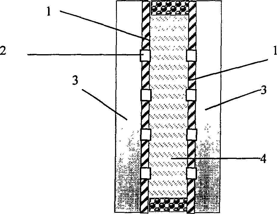
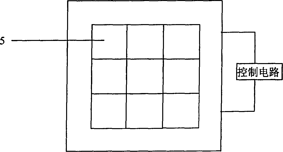
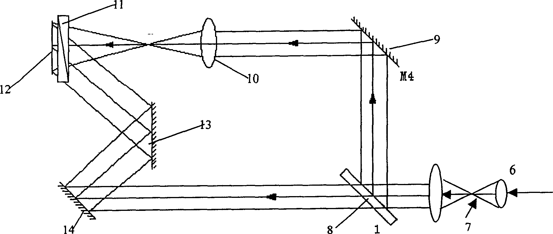
[0019] 1. Preparation of prepolymers, liquid crystal optical performance additives composed of electronically controlled polymer-dispersed liquid crystal materials, which are mixed with chemical materials such as polymers, liquid crystals, light guides, synergistic initiators, and crosslinking agents. Photopolymerization occurs under the action of a 441.6nm He-Cd laser or a 514nm Ar ion laser to form a PDLC material in which liquid crystal droplets are dispersed in a polymer matrix. Under the regulation of the electric field, the optical axis direction of the liquid crystal molecules rotates with the electric field, the effective refractive index of the liquid crystal molecules changes from different to the same as that of the polymer, and the surface of the material changes from scattering...
PUM
| Property | Measurement | Unit |
|---|---|---|
| Thickness | aaaaa | aaaaa |
Abstract
Description
Claims
Application Information
 - R&D
- Intellectual Property
- Life Sciences
- Materials
- Tech Scout
- Unparalleled Data Quality
- Higher Quality Content
- 60% Fewer Hallucinations
Browse by: Latest US Patents, China's latest patents, Technical Efficacy Thesaurus, Application Domain, Technology Topic, Popular Technical Reports.
© 2025 PatSnap. All rights reserved.Legal|Privacy policy|Modern Slavery Act Transparency Statement|Sitemap|About US| Contact US: help@patsnap.com


