Immersion lithography method and processing system

An immersion lithography and processing system technology, applied in the field of immersion lithography and its processing system, can solve problems such as uneven heat absorption and evaporation, generation problems, photoresist patterning, and adverse effects on feature size.

Inactive Publication Date: 2007-01-10
TAIWAN SEMICON MFG CO LTD
View PDF1 Cites 2 Cited by
  • Summary
  • Abstract
  • Description
  • Claims
  • Application Information

AI Technical Summary

Problems solved by technology

[0005] The immersion exposure step can use deionized water or other suitable immersion exposure liquid between the wafer and the lens. Although the exposure time is very short, the contact of the liquid with the light-sensitive layer (such as photoresist) will cause problems, such as after processing. Small droplets left behind, and / or residue from liquid and photoresist can adversely affect photoresist patterning, feature size, and other aspects. At least three different defect mechanisms have been identified
[0006] The first defect mechanism is contamination of the immersion liquid with soluble species from the photoresist, which can cause problems in subsequent processing
The second defect mechanism is that the liquid has an adverse effect on the photoresist, causing uneven heat absorption and evaporation during post-exposure baking, which will cause different temperature distributions in different parts of the wafer
The third defect mechanism is that the liquid diffuses into the photoresist and limits the chemical amplification reaction (CAR) used in the subsequent photolithography process

Method used


Image

  • Immersion lithography method and processing system
  • Immersion lithography method and processing system
  • Immersion lithography method and processing system

Examples


Embodiment Construction

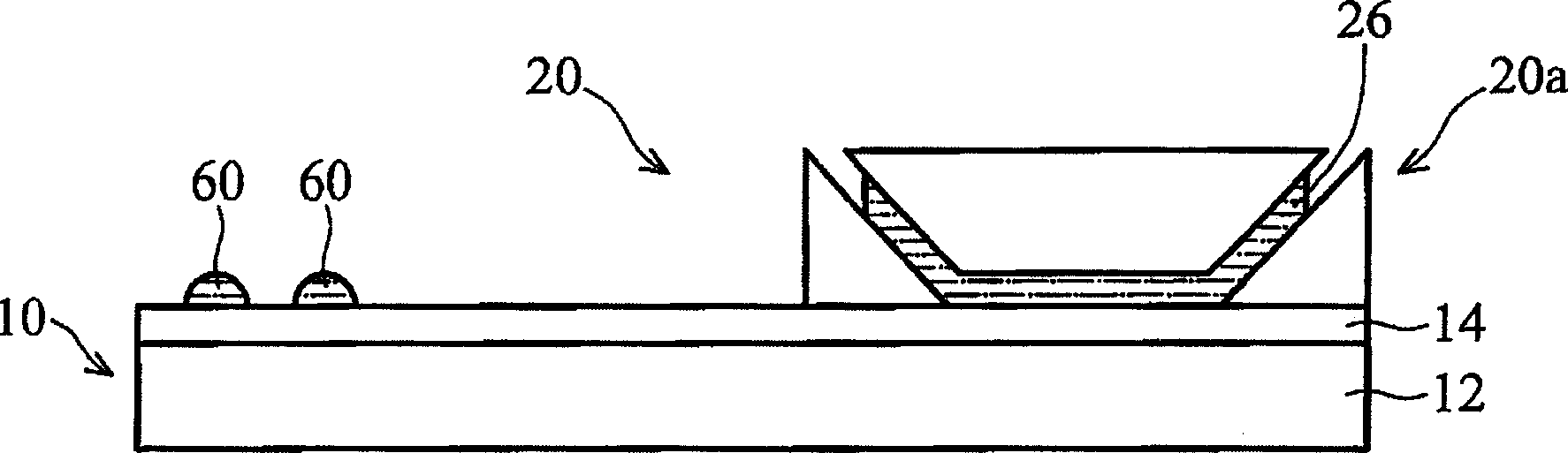
[0041] see figure 1 The semiconductor wafer 10 includes a base 12 and a patterned layer 14 , the base 12 is a structure of one or more layers, including polysilicon, metal and / or dielectric, which will be patterned. The patterned layer 14 can be a photoresist layer, which can be patterned by an exposure process, and the wafer 10 is placed in an immersion photolithography system 20 .

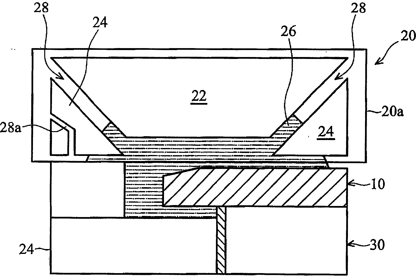
[0042] refer to figure 2 , which is an immersion lithography system 20 comprising a lens system 22; a structure 24 carrying a liquid 26 (eg, deionized water); a plurality of openings 28 through which liquid can be added or removed; and a chuck 30 for holding a wafer 10, and make the wafer move relative to the lens system 22. The liquid-carrying structure 24 and the lens system 22 constitute the immersion head 20a. The immersion head 20a can use some openings (such as the opening 28a) for air drying (air purge) to allow air to dry the wafer, while other openings are used for removal and cleanin...


PUM


Abstract

A method of performing immersion lithography on a semiconductor substrate includes providing a layer of resist onto a surface of the semiconductor substrate and exposing the resist layer using an immersion lithography exposure system. The immersion lithography exposure system utilizes a fluid during exposure and may be capable of removing some, but not all, of the fluid after exposure. After exposure, a treatment process is used to remove the remaining portion of fluid from the resist layer. After treatment, a post-exposure bake and a development step are used.

Description

technical field [0001] The invention relates to a manufacturing method of a semiconductor device, in particular to a method and system for removing photoresist residues on a semiconductor substrate. Background technique [0002] Photolithography is the technique of projecting a pattern on a mask onto a substrate such as a semiconductor wafer. In the field of semiconductor lithography technology, it is necessary to minimize the feature size of the pattern on the semiconductor wafer under the resolution limit or critical dimension, and the current critical dimension has reached below 65nm. [0003] Semiconductor photolithography generally includes coating photoresist on the top surface of a semiconductor wafer (such as a thin layer stack structure), exposing the photoresist to form a pattern; exposing the exposed photoresist and then baking it to make the polymer-based The substance is cracked; the cracked polymer photoresist is moved to the developing tank, and the exposed p...

Claims


Application Information

Patent Timeline
IPC IPC(8): G03F7/20G03F7/26H01L21/00
CPCG03F7/70341G03F7/38H01L21/0273
Inventor 张庆裕游大庆林进祥
Owner TAIWAN SEMICON MFG CO LTD
Why Eureka
Try Eureka