Fabricating method for flat display device

一种平板显示器件、制造方法的技术,应用在半导体/固态器件制造、静态指示器、电固体器件等方向,能够解决显影溶液过度损耗、工艺复杂、昂贵设备等问题

Inactive Publication Date: 2007-01-03
LG DISPLAY CO LTD
View PDF1 Cites 5 Cited by
  • Summary
  • Abstract
  • Description
  • Claims
  • Application Information

AI Technical Summary

Problems solved by technology

Thus, the process is complex
Also, the developing solution used to develop the photoresist and the photoresist pattern is excessively depleted
Moreover, expensive equipment is used in the development process of the photolithography process

Method used


Image

  • Fabricating method for flat display device
  • Fabricating method for flat display device
  • Fabricating method for flat display device

Examples


Embodiment Construction

[0031] Exemplary embodiments of the present invention will be described in detail below with reference to the accompanying drawings.

[0032] refer to Figures 3A to 8 , exemplary embodiments of the present invention are described below.

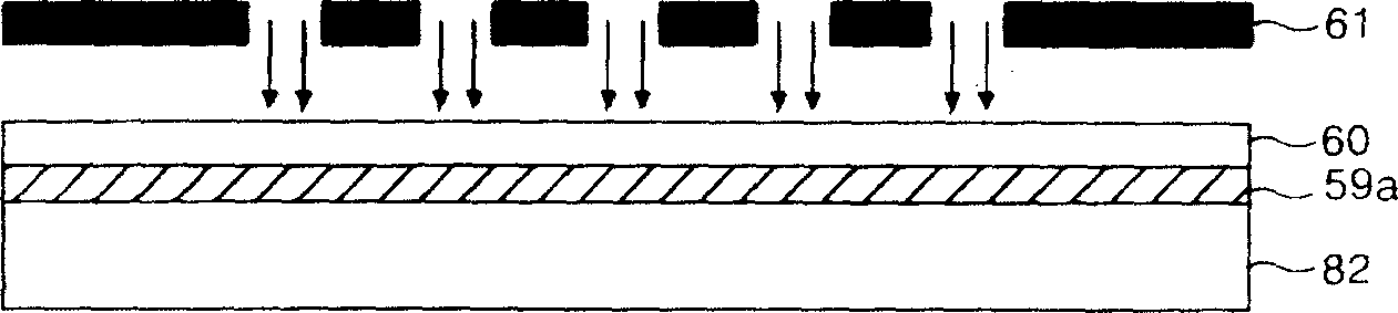
[0033] Figures 3A to 3D Shown is a cross-sectional view of a gate gradually formed according to an exemplary embodiment of the present invention.

[0034] refer to Figure 3A , the nano powder gate material 159a is coated on the entire surface of the lower substrate 182 . The nano-gate material 159a may be a gate material such as aluminum (Al), copper (Cu), chromium (Cr), molybdenum (Mo), aluminum / neodymium (Al / Nd) or alloys thereof. The nanopowder gate material 159a may be dissolved to a nanometer (nm) size. The nanopowder gate material 159a may be dissolved in a solution.

[0035] refer to Figure 3B , the soft mold 170 is positioned on the nano-powder gate material 159a, and the soft mold 170 has a protruding portion 170b. The pr...


PUM


Abstract

A fabricating method of a flat panel display device is disclosed, which can reduce manufacturing costs of the flat panel display device. A fabricating method of a flat panel display device includes providing a conductive nanopowder thin film material having a first conductive nanopowder and a second conductive nanopowder, spreading the conductive nanopowder thin film material over a substrate, forming a conductive thin film pattern by patterning the conductive nanopowder thin film material, and forming a conductive thin film by baking the conductive thin film pattern, wherein the first conductive nanopowder is located in a middle of the conductive thin film and the second conductive nanopowder is located in an outer part of the conductive thin film.

Description

[0001] This application claims the benefit of Korean Patent Application No. 10-2005-0056553 filed June 28, 2005, which is incorporated herein by reference. technical field [0002] The invention relates to a method for manufacturing a flat panel display device. In particular, the present invention relates to a manufacturing method of a flat panel display device capable of reducing the manufacturing cost of the flat panel display device. Background technique [0003] Generally, a liquid crystal display (LCD) device controls light transmittance through liquid crystals according to video signals to display images. The liquid crystal display device may include a liquid crystal display panel, wherein the liquid crystal cells are arranged in a matrix, and a driving circuit for driving the liquid crystal display panel. [0004] Liquid crystal display devices can be classified according to the direction of the electric field driving the liquid crystal. For a liquid crystal display...

Claims


Application Information

Patent Timeline
Patent Type & Authority Applications(China)
IPC IPC(8): G02F1/133H01L21/027
CPCH01L21/76838H05K2203/0108H05K3/102H01L21/288H01L27/1214H05K2201/0272H05K3/101H05K3/04H05K2201/0257H01L27/1292Y10S977/777G02F1/136G02F1/00
Inventor 蔡基成朴美暻
Owner LG DISPLAY CO LTD
Why Eureka
Try Eureka