Fast response broad frequency range laser detector made of hetero-junctions material
A laser detector and fast-response technology, applied in the field of laser detectors, can solve the problems of inability to detect and measure the laser pulse pulse laser waveform, the response band is not wide enough, and the light response of the detector is not fast enough.
- Summary
- Abstract
- Description
- Claims
- Application Information
AI Technical Summary
Problems solved by technology
Method used
Image
Examples
Embodiment 1
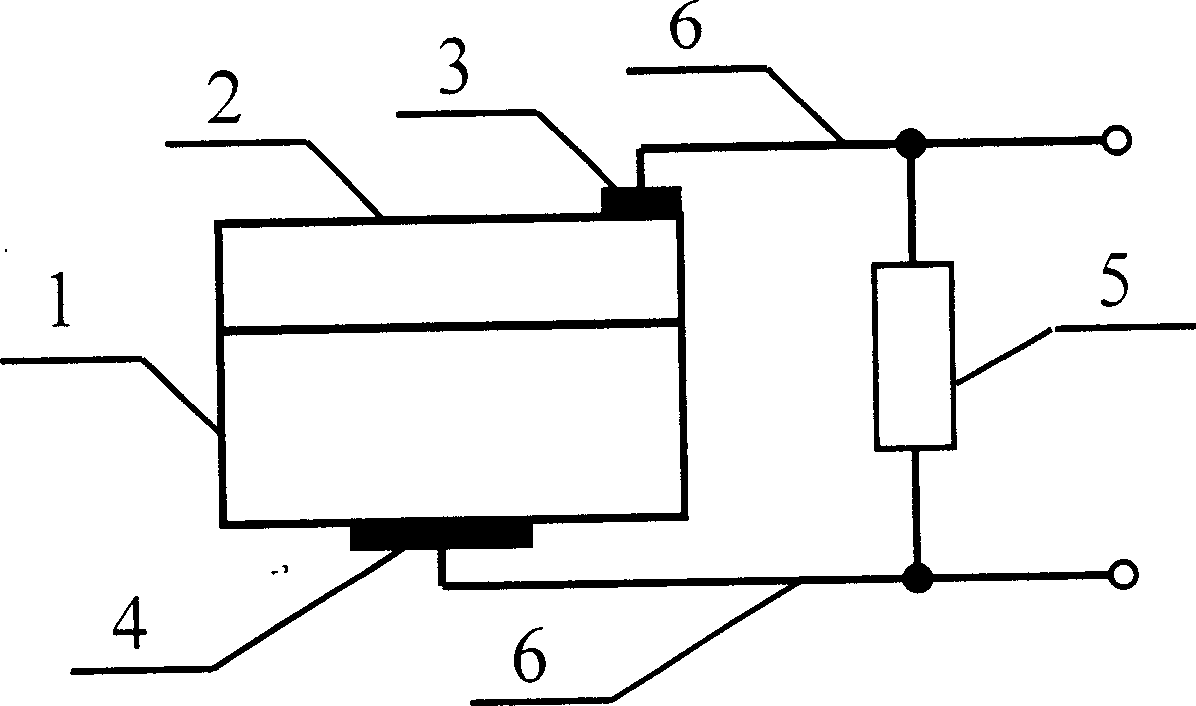
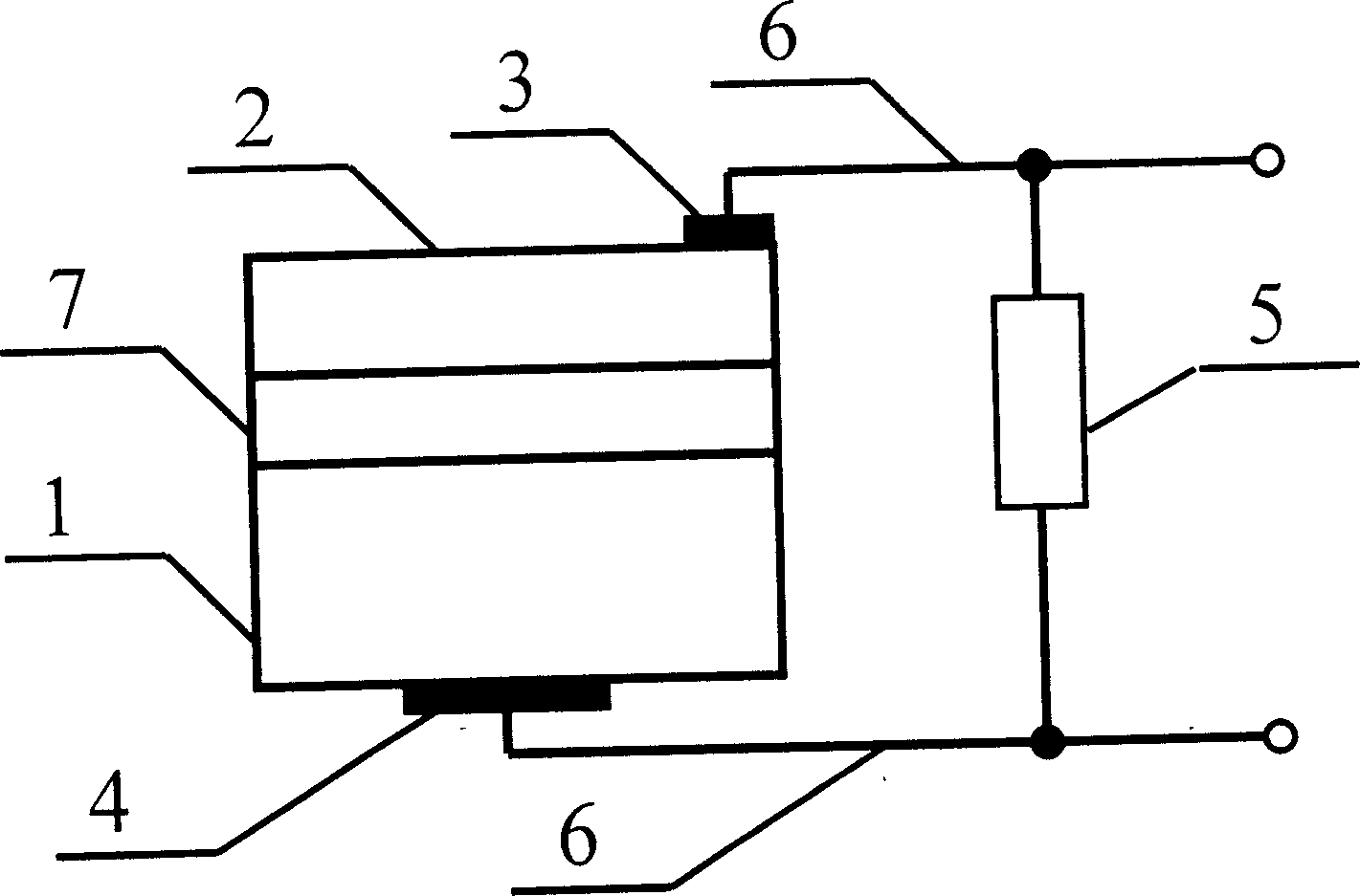
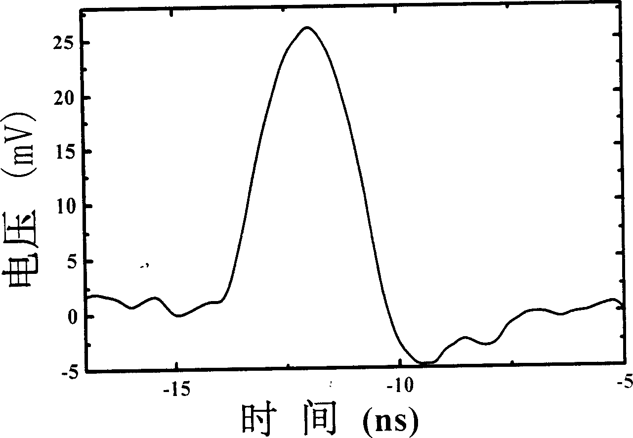
[0023] refer to figure 1 , to prepare a laser detector with a silicon-doped lanthanum manganate two-layer structure, and prepare it in conjunction with the specific manufacturing process below: to describe in detail the structure of the fast-response broadband laser detector made of heterojunction materials in the present invention, select laser molecules Beam epitaxy equipment, the substrate is an n-type silicon wafer 1, on which a 300nm-thick, p-type La 0.7 Sr 0.3 MnO 3 Photoresponsive material layer 2, forming La 0.7 Sr 0.3 MnO 3 / Si two-layer heterostructure sample, cut into a size of 1 × 1 cm 2 The detector core; use hydrofluoric acid to remove the silicon oxide on the silicon surface, weld the second electrode 4 of about φ2mm on the silicon surface with indium, and use indium on the La 0.7 Sr 0.3 MnO 3 Weld the first electrode 3 of about φ1mm on the surface of one corner of the film; use two φ0.1mm copper wires as electrode leads 6, and weld one end of the two φ0...
Embodiment 2
[0027] Laser molecular beam epitaxy equipment was selected to directly epitaxially grow 100nm thick, p-type La 0.7 Sr 0.3 MnO 3 Thin film photoresponsive material layer 2, prepared La 0.7 Sr 0.3 MnO 3 The / Si two-layer heterostructure sample is used as a chip, and a 2-inch chip is used to assemble the laser detector with the same two-layer structure as in Example 1.
Embodiment 3
[0029]Using a laser molecular beam epitaxy device, a layer of SrO was used as a buffer layer to epitaxially grow 800nm thick La on n-type silicon. 0.95 Ba 0.05 MnO 3 Thin film photoresponsive material layer 2, forming La 0.95 Ba 0.05 MnO 3 / Si two-layer heterostructure chip, in La 0.95 Ba 0.05 MnO 3 One edge of the thin film layer is vacuum-evaporated with a 0.5 mm wide platinum first electrode 3, and the rest is the same as the fast-response broadband laser detector made of heterojunction materials prepared according to Example 1.
PUM
 Abstract
Description
Claims
Application Information
 - Generate Ideas
- Intellectual Property
- Life Sciences
- Materials
- Tech Scout
- Unparalleled Data Quality
- Higher Quality Content
- 60% Fewer Hallucinations
Browse by: Latest US Patents, China's latest patents, Technical Efficacy Thesaurus, Application Domain, Technology Topic, Popular Technical Reports.
© 2025 PatSnap. All rights reserved.Legal|Privacy policy|Modern Slavery Act Transparency Statement|Sitemap|About US| Contact US: help@patsnap.com


