
Vertical structure semiconductor chip or device growthing on silicone substrate

A vertical structure and growth substrate technology, applied in the direction of semiconductor devices, electrical components, circuits, etc., can solve the problem of epitaxial layer growth rate and composition ratio changes, epitaxial layer uneven electrical/optical characteristics, and silicon wafer surface temperature unevenness and other issues, to achieve the effect of improving light extraction efficiency, uniform current distribution, and strong antistatic ability

Inactive Publication Date: 2005-10-26
金芃
View PDF0 Cites 18 Cited by
  • Summary
  • Abstract
  • Description
  • Claims
  • Application Information

AI Technical Summary

Problems solved by technology

First, small temperature fluctuations will cause significant changes in the growth rate and composition ratio of the epitaxial layer, thus causing the inhomogeneity of the electrical / optical properties of the epitaxial layer
Second, because the upper surface of the silicon wafer radiates heat energy and the gas contacting the upper surface of the silicon wafer absorbs heat energy, during the epitaxial growth process, the edge of the silicon wafer is lifted upwards, which causes the temperature on the surface of the silicon wafer to be unevenly distributed in the radial direction , and cause the electrical / optical properties of the epitaxial layer to be radially inhomogeneous
Uniformity issues limit diameter of silicon growth substrates that can be used

Method used


Image

  • Vertical structure semiconductor chip or device growthing on silicone substrate
  • Vertical structure semiconductor chip or device growthing on silicone substrate
  • Vertical structure semiconductor chip or device growthing on silicone substrate

Examples


Embodiment

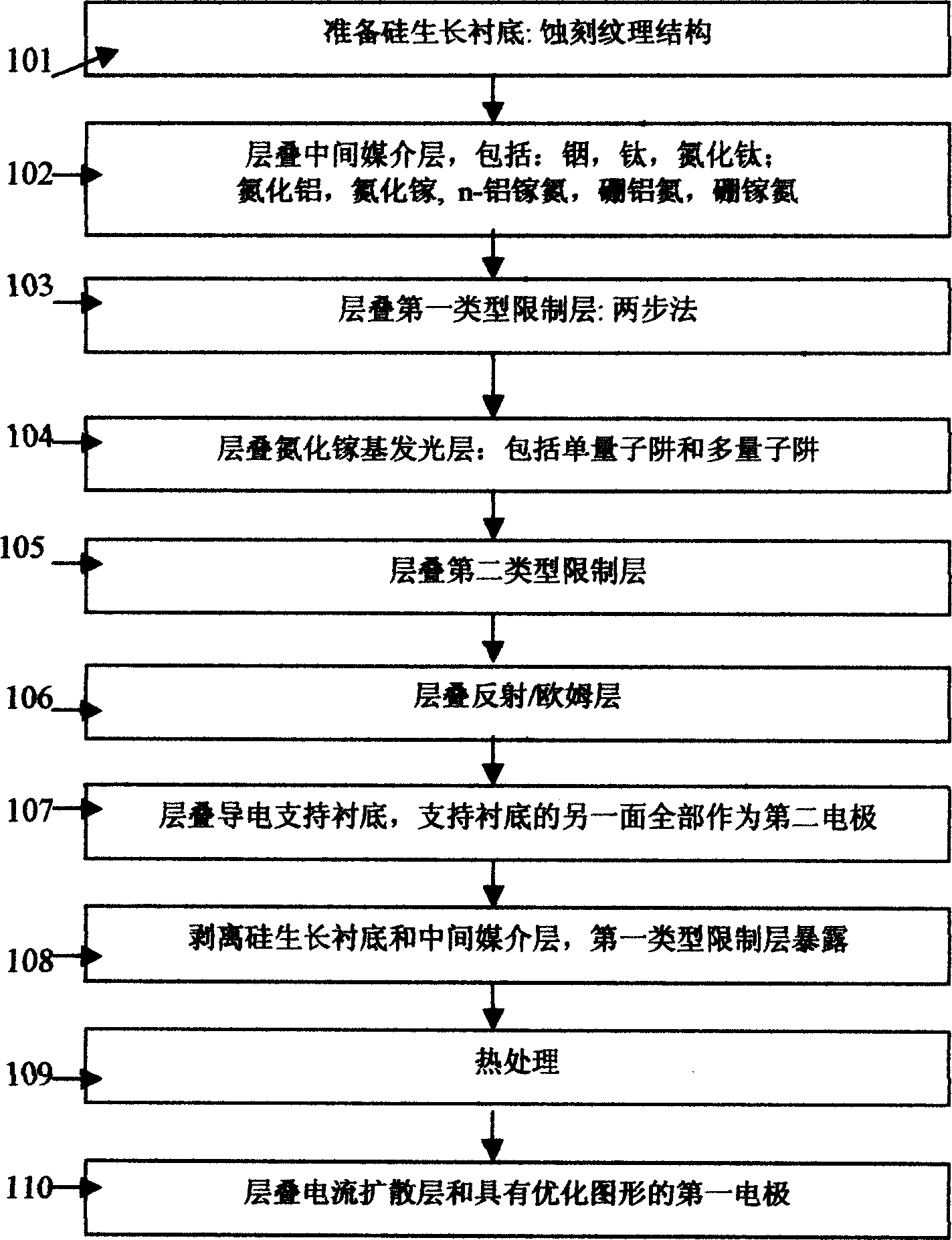
[0031] (4) One side of the growth substrate of the present invention may have a textured structure formed by etching. Etching methods include wet and dry methods. A specific implementation example of wet chemical etching: using NHO 3 and HF solution to etch silicon wafers. A specific implementation example of dry etching: plasma etching.

[0032] (5) In order to prevent the edge of the silicon growth substrate of the present invention from warping upward during epitaxial growth, the following methods can be used, but not limited to: (1) non-rigidly fixing the silicon growth substrate on a thermally conductive surface on the tray. Materials for the pallet include, but are not limited to, molybdenum. Methods of non-rigid fixation include, but are not limited to, low melting point metal bonding, non-rigid mechanical clamps, or a combination of both. (2) Using an infrared heat source to heat the upper surface of the silicon wafer growth substrate. (3) Silicon wafers have hig...


PUM


Abstract

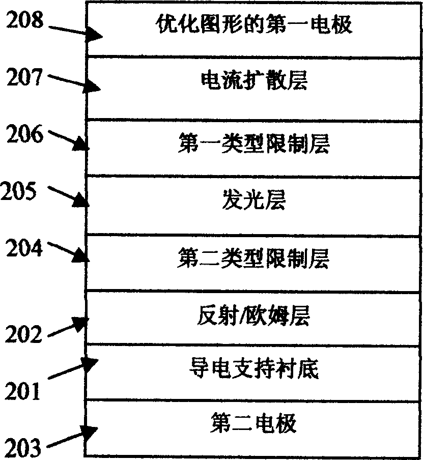
This invention discloses a vertical semiconductor chip (including LEDS of GaN base and Galn PN BASE) and its batch production method including the following steps: laminating an intermediate medium layer on a silicon grow substrate, laminating a first kind limit layer on the medium layer, laminating a light emitting layer and a second kind limit layer on the first limit layer, laminating reflection / ohm layer on the second kind limit layer, laminating a conduction layer supporting the substrate on the reflection / ohm layer, stripping the grown substrate and the intermediate layer to expose the first limit layer, laminating a current diffusion layer on the first kind limit layer, laminating a first electrode with optimized patterns on the current diffusion layer.

Description

technical field [0001] The invention discloses a high-quality vertical structure gallium nitride-based semiconductor light-emitting diode grown on a large-diameter silicon substrate and the technology and process of growing it on a silicon wafer, belonging to the field of semiconductor electronics technology. Background technique [0002] High-power semiconductor light-emitting diodes have great prospects to replace incandescent lamps, but first, technical problems must be solved. The main problems include low light extraction efficiency, low heat dissipation efficiency, and high production costs. [0003] In order to solve the heat dissipation problem of high-power GaN-based semiconductor light-emitting diodes with a lateral structure, flip-chip bonding technology was proposed. However, the flip-chip technology is complex in process and high in cost. Therefore, a large amount of research has been devoted to a gallium nitride-based semiconductor light-emitting diode with a ...

Claims


Application Information

Patent Timeline
Patent Type & Authority Applications(China)
IPC IPC(8): H01L33/00H01L33/06
Inventor 彭晖彭一芳
Owner 金芃
Learn More