Manufacture of semiconductor device
A manufacturing method and semiconductor technology, applied in the direction of semiconductor/solid-state device manufacturing, transistors, electrical components, etc., to achieve the effect of suppressing the increase of resistance value
- Summary
- Abstract
- Description
- Claims
- Application Information
AI Technical Summary
Problems solved by technology
Method used
Image
Examples
no. 1 Embodiment approach
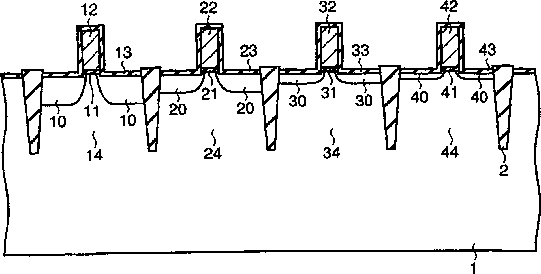
[0038] figure 1 It is a main part of the semiconductor device according to the first embodiment of the present invention, and is a cross-sectional view showing a low-concentration impurity region before forming a deep source and a deep drain. A part of this low-concentration impurity region becomes a low-concentration impurity region thereafter.
[0039] In this embodiment mode, low-concentration impurity regions 10 , 20 , 30 , and 40 having different junction depths are formed on the same semiconductor substrate (for example, Si substrate) 1 . The knot depth satisfies the relationship of 10>20>30>40.
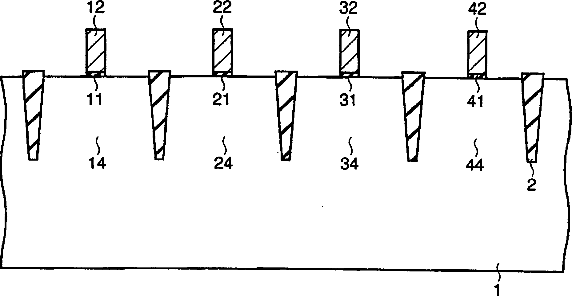
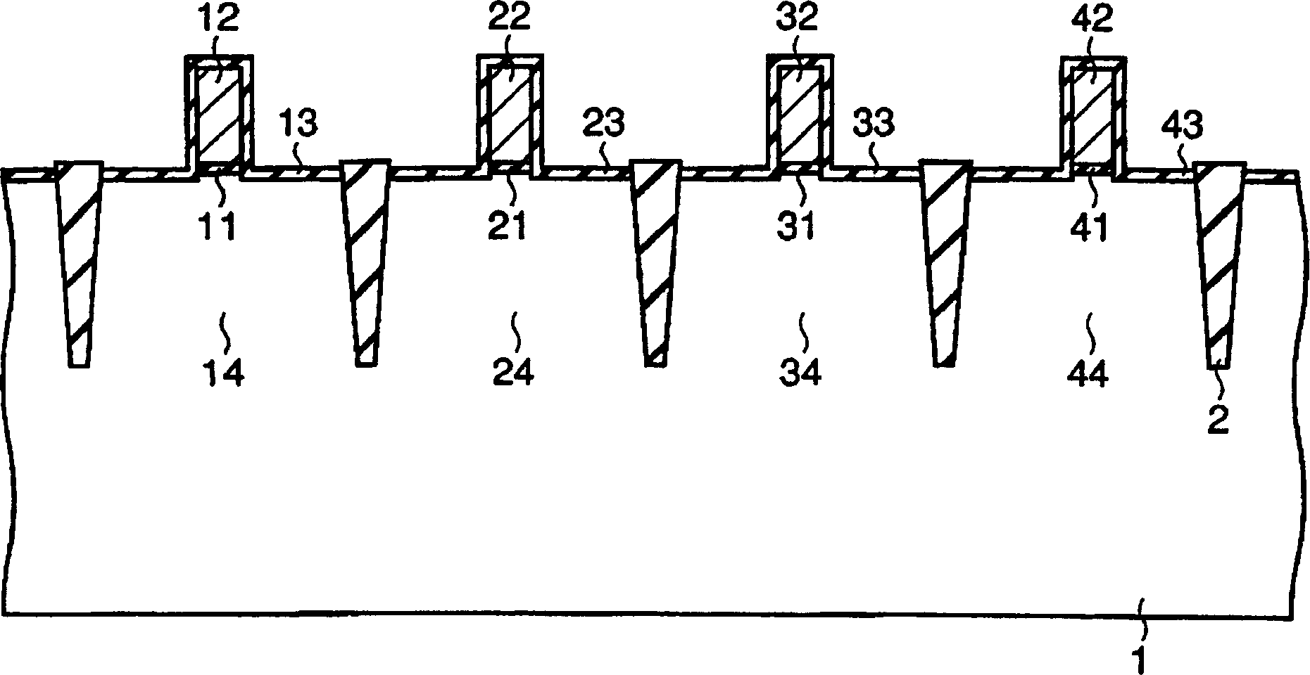
[0040] On the surface of the semiconductor substrate 1, an element isolation region 2 is formed by, for example, an STI (Shallow Trench Isolation: Shallow Trench Isolation) method in order to isolate and form the element regions 14, 24, 34, and 44 of the respective MOS transistors. Thus, the element regions 14 , 24 , 34 , and 44 are formed. The element isolation region 2 is ...
no. 2 Embodiment approach
[0064] Figure 13 It is a sectional view showing main parts of the semiconductor device according to the second embodiment of the present invention.
[0065] In this embodiment mode, low-concentration impurity regions 10 , 20 , 50 , and 60 having different junction depths are formed on the same semiconductor substrate 1 . The knot depth satisfies the relationship of 10>20>50. In addition, low-concentration impurity region 50 and low-concentration impurity region 60 have substantially the same junction depth.
[0066] The low-concentration impurity region 50 and the low-concentration impurity region 60 differ in the depth of the concentration peak during impurity ion implantation (hereinafter referred to as the peak depth of implanted impurity concentration). Figure 14 It is a graph showing the peak depths of implanted impurity concentrations in the low-concentration impurity region 50 and the low-concentration impurity region 60 . exist Figure 14 In , the dotted line ind...
PUM
 Abstract
Description
Claims
Application Information
 - R&D
- Intellectual Property
- Life Sciences
- Materials
- Tech Scout
- Unparalleled Data Quality
- Higher Quality Content
- 60% Fewer Hallucinations
Browse by: Latest US Patents, China's latest patents, Technical Efficacy Thesaurus, Application Domain, Technology Topic, Popular Technical Reports.
© 2025 PatSnap. All rights reserved.Legal|Privacy policy|Modern Slavery Act Transparency Statement|Sitemap|About US| Contact US: help@patsnap.com


