Semiconductor device and method for making same

A manufacturing method and semiconductor technology, applied in semiconductor/solid-state device manufacturing, semiconductor devices, transistors, etc., can solve problems such as inability to operate transistors, deterioration of transistor characteristics, deviation of gate electrode resistance, etc., achieve high yield, and prevent carbon pollution , the effect of suppressing in-plane deviation

Inactive Publication Date: 2005-05-04
SANYO ELECTRIC CO LTD
View PDF4 Cites 4 Cited by
  • Summary
  • Abstract
  • Description
  • Claims
  • Application Information

AI Technical Summary

Problems solved by technology

[0021] However, wafers obtained by growing thin silicon crystals on insulators, such as wafers with SOI (Silicon On Insulator) structures that have been developed and used in recent years, pose a very serious problem.
Since the thickness of silicon-on-insulator is about 50nm to 100nm, it is very thin, so if Figure 15 As shown, the silicon reduction of 34nm will lead to a large reduction in the depth of the impurity region or silicide layer
As a result, the characteristics of the transistor deteriorate
Sometimes the impurity region or silicide layer of the depth necessary for the operation of the transistor cannot be obtained, so the transistor cannot be operated
[0022] In addition, during dry etching, variations in the etching rate and selectivity will occur depending on the position in the wafer plane. As a result, there is also a problem that the resistance of the source, drain region, or gate electrode in the wafer plane is generated. deviation

Method used


Image

  • Semiconductor device and method for making same
  • Semiconductor device and method for making same
  • Semiconductor device and method for making same

Examples


Embodiment Construction

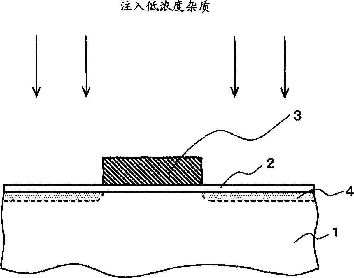
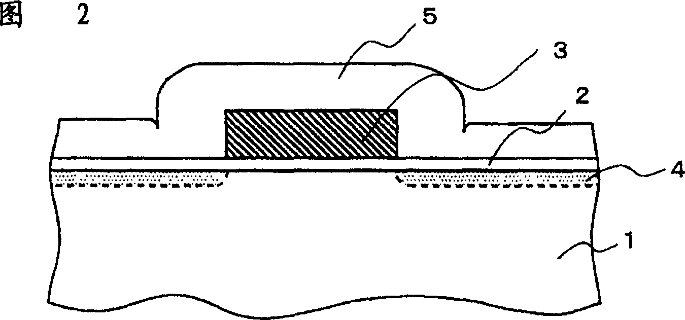
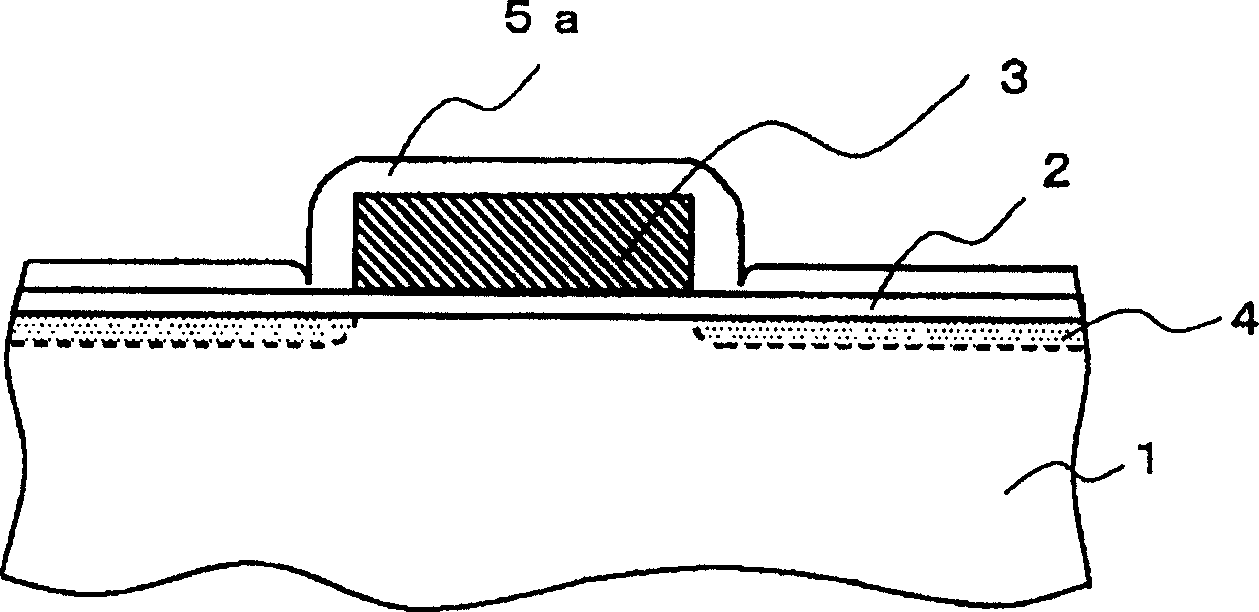
[0042] refer to figure 1 ˜ FIG. 8 illustrate the manufacturing method of the semiconductor device of the present invention.

[0043] refer to figure 1 A silicon oxide film obtained by a thermal oxidation method with a film thickness of about 5 nm was formed on the silicon substrate 1 . This is used as the gate insulating film 2 . Further, a polysilicon film having a film thickness of approximately 200 nm is formed on the gate insulating film 2 . This is processed by photolithography and etching to form gate electrode 3 .

[0044] In addition, although not shown, there is also a method of forming a silicon oxide film or the like on the polysilicon film and using it as a hard mask in order to perform etching with excellent precision.

[0045] Then, using the gate electrode 3 as a mask, for example, phosphorous ions can be used, and the implantation dose is 1 to 5×10 14 (Number of ions / cm 2 ) level of low-concentration impurity, forming low-concentration impurity region 4...


PUM

PropertyMeasurementUnit
coating thicknessaaaaaaaaaa

Abstract

Disclosed is a manufacturing method of a semiconductor device. An LDD structure and a silicide layer are formed without a reduction in thickness of a silicon substrate or a carbon contamination. Forming a spacer on a sidewall of a gate electrode is performed in two process steps, i.e. dry-etching and wet-etching. Also, a silicon nitride film used as a buffer film in injection of high dose of impurities is removed by wet-etching. As a result, the reduction in thickness of the silicon substrate and the carbon contamination can be prevented. In addition, variation in depth of the high and low impurity concentration regions and silicide forming region with locations on the wafer can be suppressed because of high selection ratio available with the wet-etching.

Description

technical field [0001] The present invention relates to a manufacturing method of a semiconductor device, in particular to a manufacturing method of a semiconductor device having an LDD (Lightly Doped Drain) structure and forming a silicide layer on a silicon substrate or a gate electrode. Background technique [0002] With the advancement of miniaturization of semiconductor devices, there arises a problem that the characteristics of MOS transistors are degraded by the short channel effect. In response to this, a technology called an LDD (Lightly Doped Drain) structure has been developed and utilized. In addition, reducing the size of the gate electrode, source, and drain regions also raises the problem of increased resistance of the gate electrode, source, and drain regions. As a method to deal with this problem, a silicide layer called metal silicide (Silicid) is used in which a silicide layer obtained by reacting silicon and a transition metal is formed by self-alignment...

Claims


Application Information

Patent Timeline
Patent Type & Authority Applications(China)
IPC IPC(8): H01L21/02H01L21/265H01L21/28H01L21/336H01L21/8234H01L21/84H01L29/78
CPCH01L29/7833H01L21/2652H01L29/665H01L29/6659
Inventor 饭塚胜彦冈田和央森智典土桥博之铃木弘之本多孝好谷口敏光
Owner SANYO ELECTRIC CO LTD
Why Eureka
Try Eureka