Mold type semiconductor laser

A technology for molding semiconductors and lasers, which is applied to semiconductor lasers, structural details of semiconductor lasers, semiconductor devices, etc., and can solve problems such as high price, high difficulty, and increased cost

Inactive Publication Date: 2005-02-02
ROHM CO LTD
View PDF2 Cites 1 Cited by
  • Summary
  • Abstract
  • Description
  • Claims
  • Application Information

AI Technical Summary

Problems solved by technology

In such a tank-shaped structure, it is necessary to use an expensive stem forged by cold forging. At the same time, in order to correct astigmatism, the cylindrical cover must be formed into a special shape cut into a bevel, and there is a problem that the price is very high.
In particular, in order to correct the astigmatism, it is necessary to strictly set the angle of the laser emission direction and the thickness of the parallel transparent plate according to the astigmatism of the laser light emitted by the laser sheet. Attention must also be paid to the rotation, etc., which will greatly increase the cost
Moreover, in the tank structure, due to the increase in the number of parts, the number of processes also increases, and it is necessary to use a difficult method, and there are also problems such as a decrease in yield.
[0006] On the other hand, in a structure using a lead frame, that is, a device called a lead frame structure, such as Figure 7 As shown, although there is a structure in which an optical spacer is attached to the end surface of the mold resin, if a single transparent plate or a circular polarizing plate (optical spacer) is arranged, even if the end surface of the resin is not flat and slightly Tilting will not affect it, but the end faces of the molded resin cannot be completely consistent with the upper molding resin and the lower molding resin, and a step will be generated at the interface, and the circular polarizing plate attached to the end face will be inclined. To correct the above-mentioned astigmatism, it is necessary to strictly configure the parallel transparent plate, that is, the parallel transparent plate has a predetermined thickness, and is at right angles to the semiconductor lamination layer of the laser chip, and is inclined from 90 degrees to the axial direction of the laser beam. However, there is a problem that the desired characteristics cannot be obtained when the structure is applied to the upper mold resin and the lower mold resin.

Method used


Image

  • Mold type semiconductor laser
  • Mold type semiconductor laser
  • Mold type semiconductor laser

Examples


Embodiment Construction

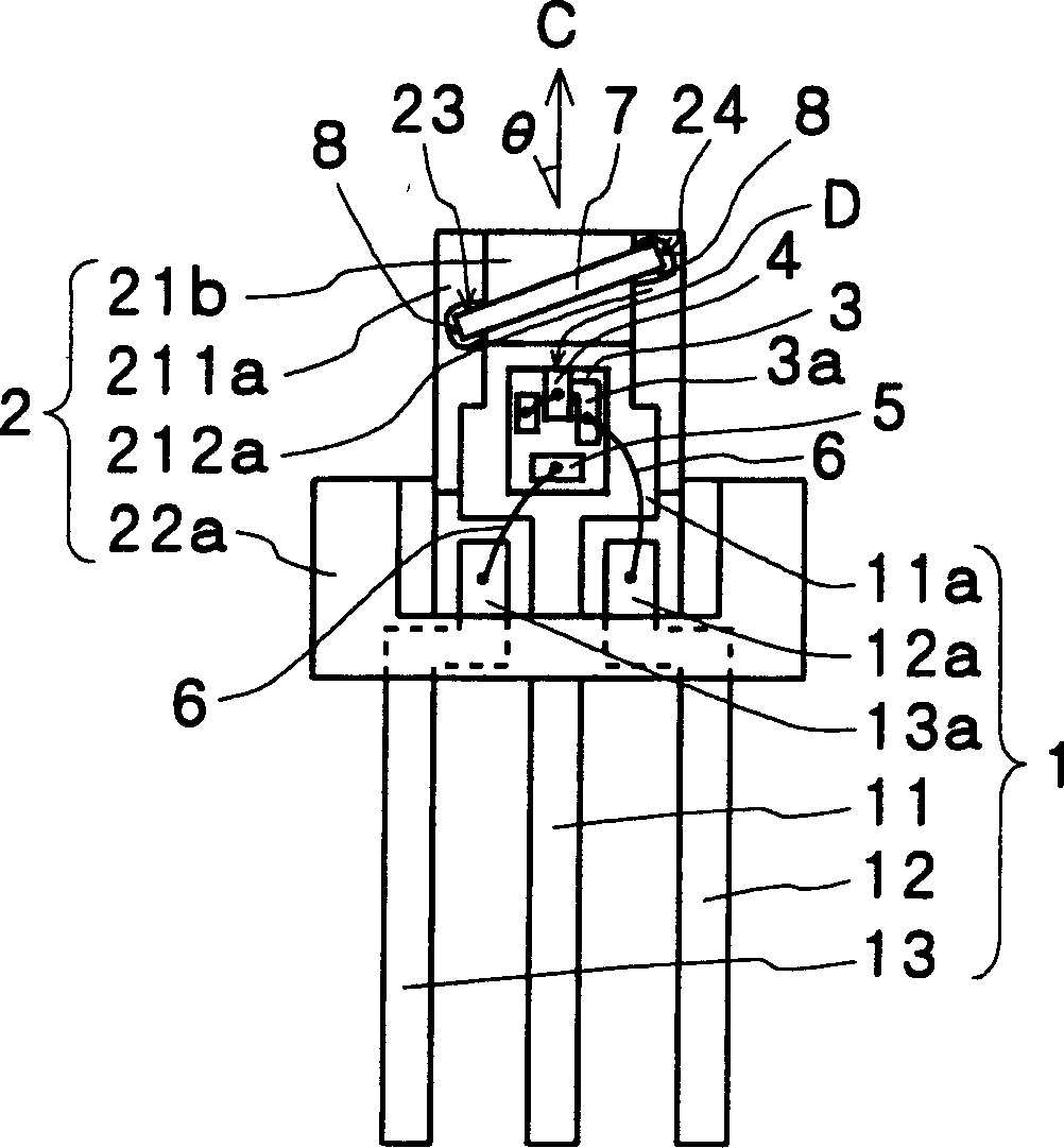
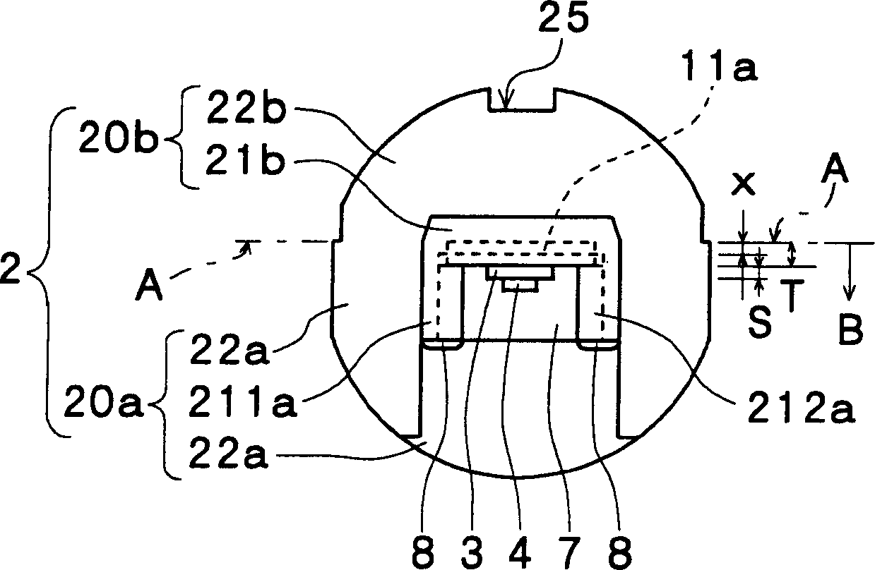
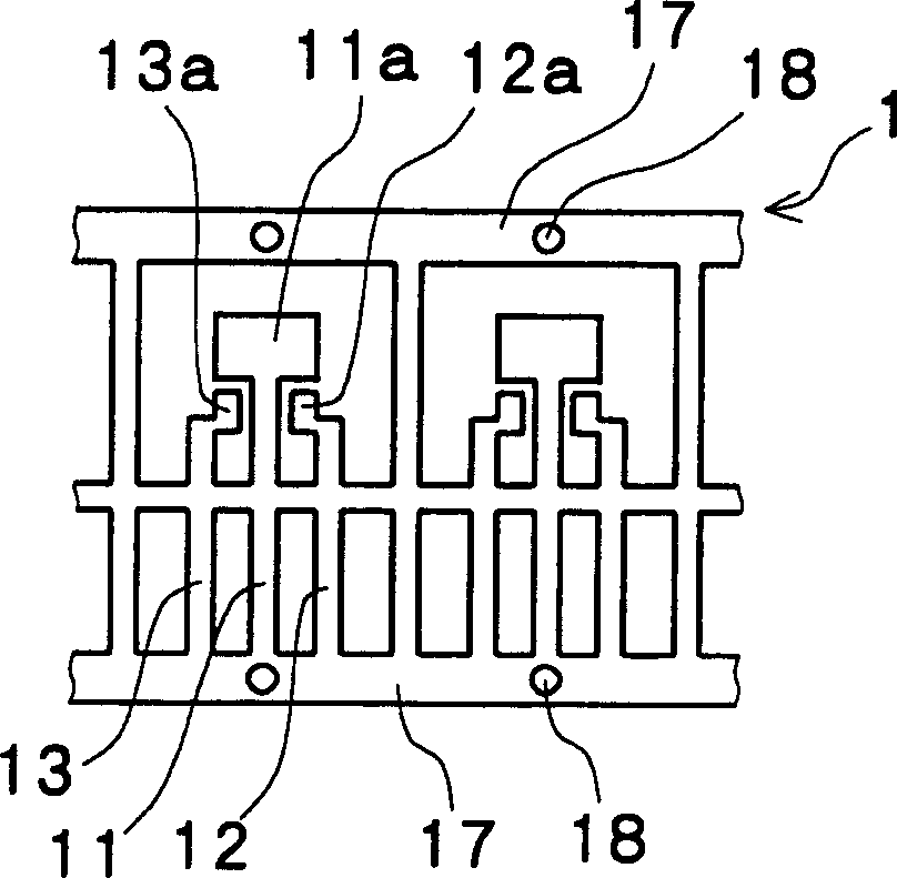
[0021] Embodiments of the molded semiconductor laser of the present invention will be described below with reference to the drawings. An explanatory diagram of a front view and a top view of an embodiment of the molded semiconductor laser of the present invention is shown in Figure 1A-1B . As shown in the drawing, a die pad 11a formed of a plate-shaped lead frame body 1 and a plurality of leads 11 to 13 are integrally held in a package 2 made of molded resin. The laser chip 4 is mounted on the die pad 11 a through the sub-mount 3 . Further, slits 23 and 24 for forming parallel transparent plate 7 in package 2 at a predetermined angle θ for correcting astigmatism, which are not perpendicular to laser beam emission direction C, are fixed in front of emission surface D of laser chip 4 . In addition, θ is the angle formed by the parallel transparent plate 7 with respect to the plane perpendicular to the emission direction C of the laser beam, that is, the angle formed by the no...


PUM


Abstract

Mold type semiconductor laser. A laser chip is mounted on a die pad with respective leads being secured thereto through a package. The package includes a body portion which has at least an upper mold resin portion that covers the upper face side (B) with respect to a lower face of the die pad serving as a parting line (A); and two frame side walls, which extend in a direction parallel to the laser-beam outgoing direction (C) of the laser chip, and also extend ahead of the laser chip outgoing face (D) on both sides with the laser chip interposed therebetween. Slits are formed in each of the two frame side walls not in a direction perpendicular to the outgoing direction of the laser beam, but with a predetermined angle for correcting astigmatism, and transparent plate (7) is secured to the slits. Consequently, it is possible to provide a semiconductor laser for use in an optical disk, which has an inexpensive structure using not a can-type structure, but a lead frame and mold resin, and is capable of positively correcting astigmatism.

Description

technical field [0001] The present invention relates to a compact and low-cost manufacturing structure having a light source for pickup particularly suitable for CD, DVD (digital versatile disk), DVD-ROM, and data-writable CD-R / RW. A semiconductor laser. More specifically, it relates to a molded semiconductor laser with a structure capable of correcting astigmatism at low cost by forming a resin package instead of the conventional can type covered with a metal cover. Background technique [0002] A stem type semiconductor laser capable of preventing astigmatism, which has been used in pickups for CDs and the like, has such Image 6 structure shown. That is to say, metal materials such as iron are formed by cold forging, a part of the central part of the base 21 is lifted to form the heat sink part 22, and the stem 20 with the wires 23 and 25 fixed by the glass 26 is used. ) 31 is mounted on the heat sink portion 22 through a submount (submount) 34 made of a silicon substra...

Claims


Application Information

Patent Timeline
Patent Type & Authority Applications(China)
IPC IPC(8): G11B7/125G11B7/12G11B7/123G11B7/135G11B7/1365G11B7/1392H01S3/04H01S5/00H01S5/02H01S5/0232H01S5/0683
CPCH01S5/0683H01S5/02244H01S5/02212G11B7/1205G11B7/1365H01S5/02296G11B7/13922G11B7/123H01L2224/48091H01L2224/48247H01L2224/45144H01S5/0231H01S5/02257H01S5/0232H01L2924/00014H01L2924/00
Inventor 山本刚司
Owner ROHM CO LTD
Why Eureka
Try Eureka