Oxide film forming method

A technology of oxide film and oxidation method, which is applied in the direction of electrical components, semiconductor/solid-state device manufacturing, circuits, etc., can solve the problems of uneven film thickness, difficult modification, low reliability of oxide film, etc., and achieve high-quality results

Inactive Publication Date: 2004-08-04
TOKYO ELECTRON LTD
View PDF0 Cites 3 Cited by
  • Summary
  • Abstract
  • Description
  • Claims
  • Application Information

AI Technical Summary

Problems solved by technology

However, especially when forming an oxide film with a final film thickness of 2 nm or less, the proportion of the protective oxide film on the finally obtained oxide film is large, so in the oxide film forming process, the protective oxide film must be fully formed. Modification is relatively difficult, and as a result, it is difficult to form a high-quality oxide film
[0016] In addition, when the formation of the protective oxide film is generally carried out in a reaction vessel or in a state where the surface temperature distribution of the wafer is uneven, the film thickness distribution of the protective oxide film formed in the wafer surface is caused by the unevenness of the surface temperature of the wafer. The non-uniformity of the film thickness distribution is very high, and as a result, the film thickness uniformity of the final oxide film is significantly reduced
[0017] (2) In the method of chemically forming a protective oxide film by wafer processing, trace metal elements are inevitably absorbed in the chemically formed protective oxide film during the wafer cleaning process, thereby becoming the final oxide film. Reasons for low reliability
However, although the degree of freedom in controlling the final film thickness increases, there is still a problem that the film thickness distribution as a protective film is caused by the unevenness of the surface temperature of the wafer due to the use of the oxide film at the time of heating. Uneven film thickness throughout
[0021] (4) In the process of heating up, the method of forming a protective oxide film with a controlled film thickness by controlling the oxygen partial pressure with nitrogen gas will inevitably cause wafer nitriding, so as already mentioned, it is difficult to form a high-quality oxide film. Oxide film
[0022] As mentioned above, there is a problem that the existing oxide film forming method cannot advantageously form a high-quality oxide film on the wafer.

Method used


Image

  • Oxide film forming method
  • Oxide film forming method
  • Oxide film forming method

Examples


Embodiment

[0126] Hereinafter, examples of the present invention will be described, but the present invention is not limited thereto.

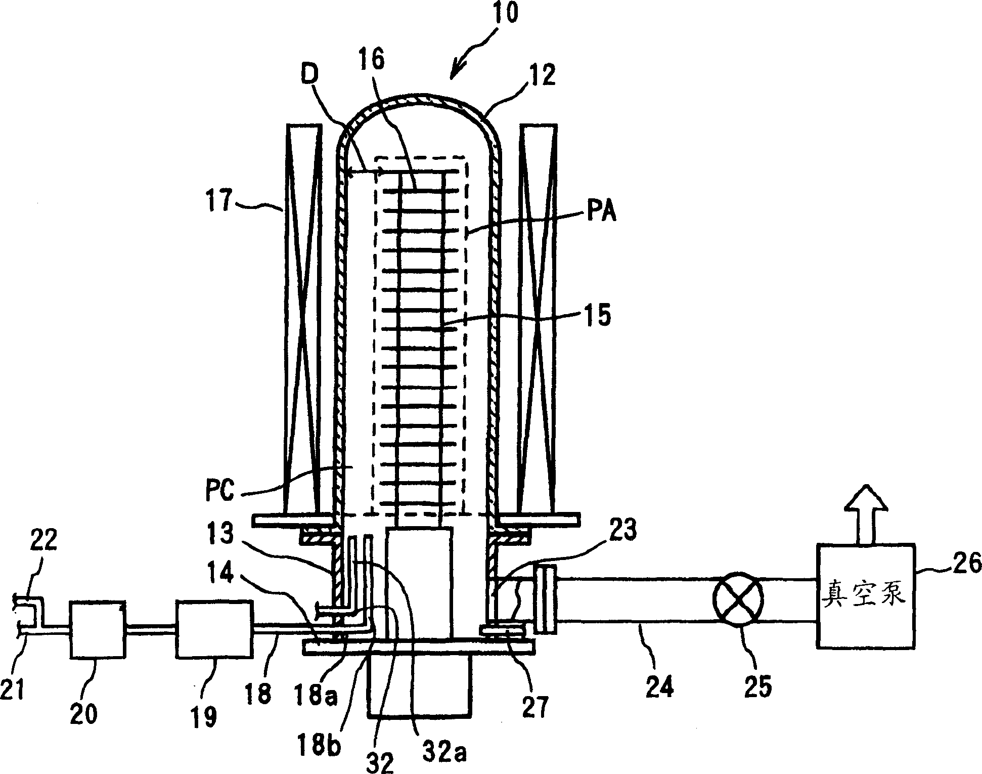
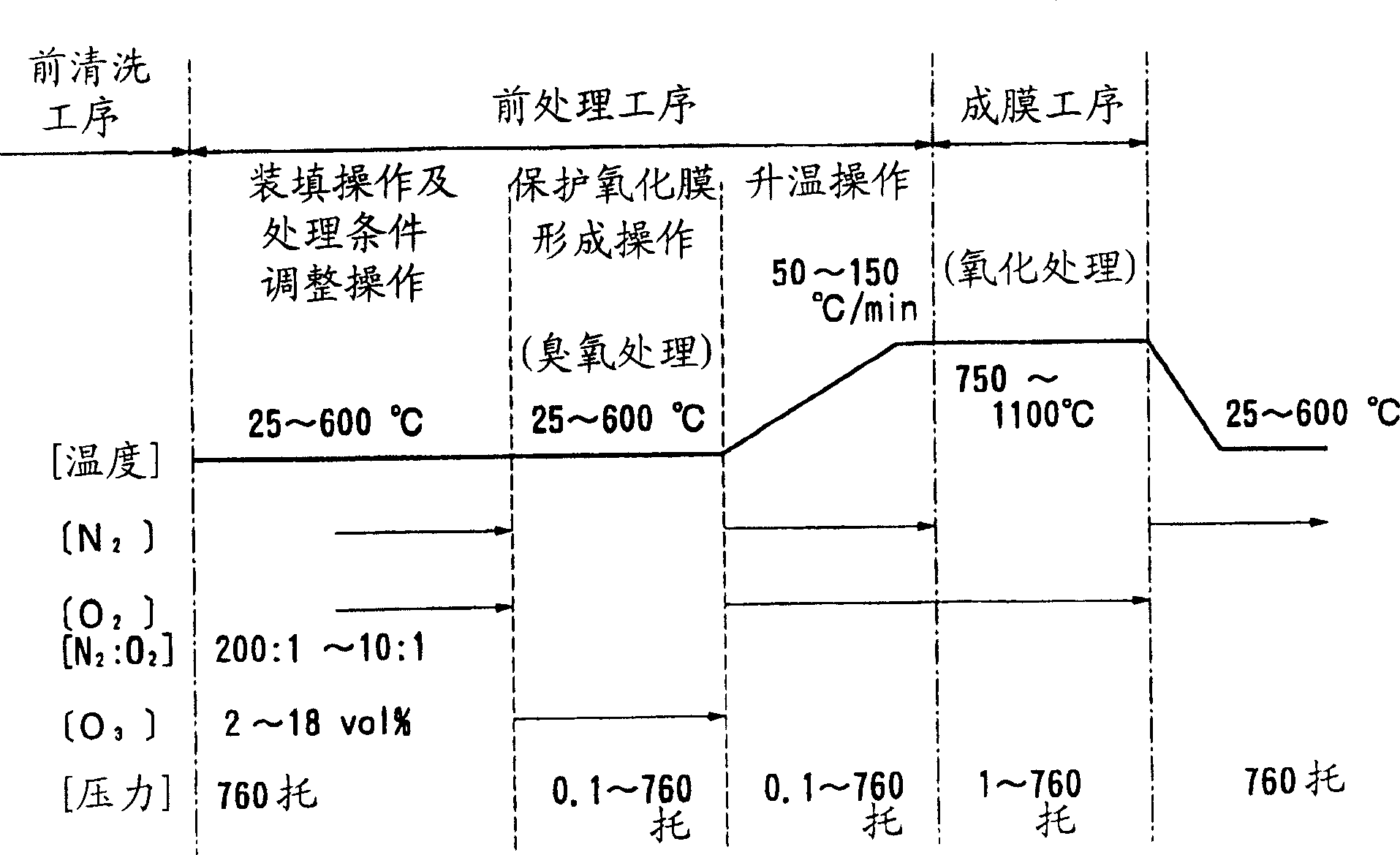
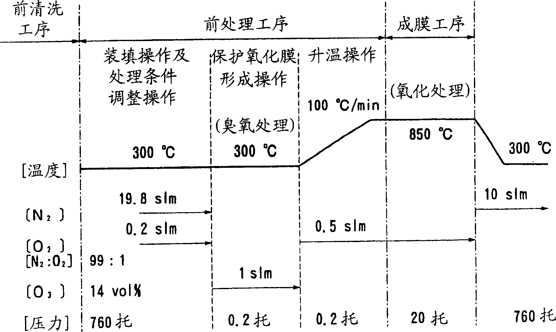
[0127] Basically using the figure 1 The oxidation treatment device of the shown structure, according to image 3 The sequence chart shown implements the following steps.

[0128] [Pre-cleaning process]

[0129] An overetching treatment of 30% of the film thickness of the sacrificial oxide film on a silicon wafer having a diameter of 8 inches was performed in an aqueous hydrofluoric acid solution having a concentration of 1 vol % at a temperature of 23°C.

[0130] [Pre-treatment process]

[0131] (1) Loading operation

[0132] The 100 wafers obtained in the pre-cleaning process were held on a quartz wafer boat 15, placed on the cover 14, and nitrogen gas was supplied to the reaction processing chamber PC at a ratio of 19.8 slm of nitrogen and 0.2 slm of oxygen. and oxygen, the temperature in the reaction processing chamber PC is controlled at 300°C a...


PUM


Abstract

To provide a method for the formation of oxide films to form with advantage a high-quality oxide film having excellent uniformity in film thickness and film quality over the entire wafer. The method for the formation of oxide films comprises: the pretreatment process of forming a protective oxide film on the surface of a wafer positioned in a reaction vessel by performing oxidation treatment with radical oxidative species or an atmosphere containing radical oxidative species under depressurized conditions; and the oxide-film-formation process of forming an oxide film on the wafer by performing oxidation treatment at a predetermined temperature under depressurized conditions. The oxide-film-formation process is preferably performed following the pretreatment process in a continuous manner in the reaction vessel in which the pretreatment process is performed. The pretreatment process is preferably performed at a temperature lower than the temperature for the oxide-film-formation process and also preferably performed under depressurized conditions, the level of the depressurization being higher than the level for the oxide-film-formation process. A high-quality gate-insulating film for a transistor chip can be formed according to this method for the formation of oxide films.

Description

technical field [0001] The present invention relates to an oxide film forming method for forming an oxide film on the surface of a wafer formed of, for example, silicon. Background technique [0002] In the manufacture of semiconductor devices, various treatments are performed on semiconductor wafers formed of silicon, etc., one of which is oxidation treatment to form an oxide film on the surface of the wafer. For example, it can be used for gate (gate) insulation in transistor elements. The formation of the oxide film of the film effect. In recent years, the gate insulating film has been required to be thin and have good reliability over a long period of time. [0003] The process of forming an oxide film on a wafer is performed by heating the wafer placed in a reaction vessel at a high temperature of, for example, 750 to 1100° C. in an oxygen atmosphere under normal pressure or reduced pressure. deal with. In particular, the oxide film formation method under reduced pre...

Claims


Application Information

Patent Timeline
Patent Type & Authority Applications(China)
IPC IPC(8): H01L29/78H01L21/316
CPCH01L21/02238Y10S438/909H01L21/02255H01L21/02299H01L21/31658H01L21/31662H01L21/02554H01L21/324
Inventor 菱屋晋吾秋山浩二古泽纯和青木公也
Owner TOKYO ELECTRON LTD
Why Eureka
Try Eureka