
Manufacturing method of polycrystal film and manufacturing method of oxide superconductor

A manufacturing method and oxide technology, which is applied in superconducting/high-conducting conductors, manufacturing/processing of superconducting devices, crystal growth, etc., can solve the problems of large number of necessary layers and increased manufacturing steps, etc.

Inactive Publication Date: 2004-03-03
THE FUJIKURA CABLE WORKS LTD
View PDF3 Cites 8 Cited by
  • Summary
  • Abstract
  • Description
  • Claims
  • Application Information

AI Technical Summary

Problems solved by technology

[0013] However, if Figure 12 As shown, in this four-layer structure, the number of necessary layers is large, and there is a problem of increasing manufacturing steps

Method used


Image

  • Manufacturing method of polycrystal film and manufacturing method of oxide superconductor
  • Manufacturing method of polycrystal film and manufacturing method of oxide superconductor
  • Manufacturing method of polycrystal film and manufacturing method of oxide superconductor

Examples


Embodiment

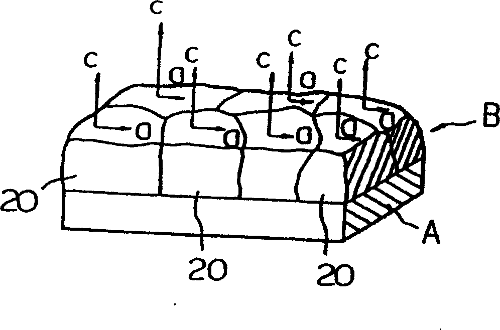
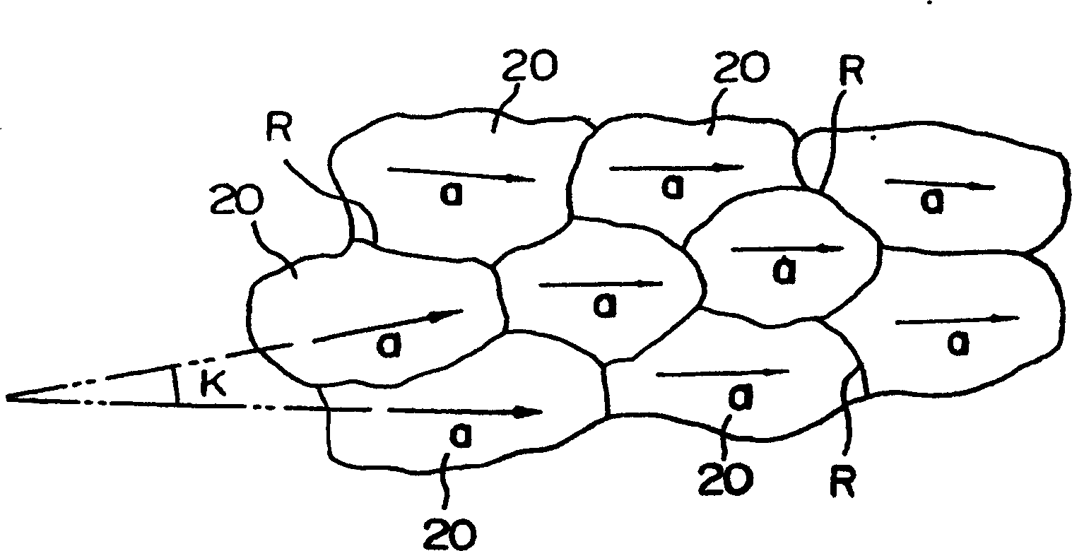
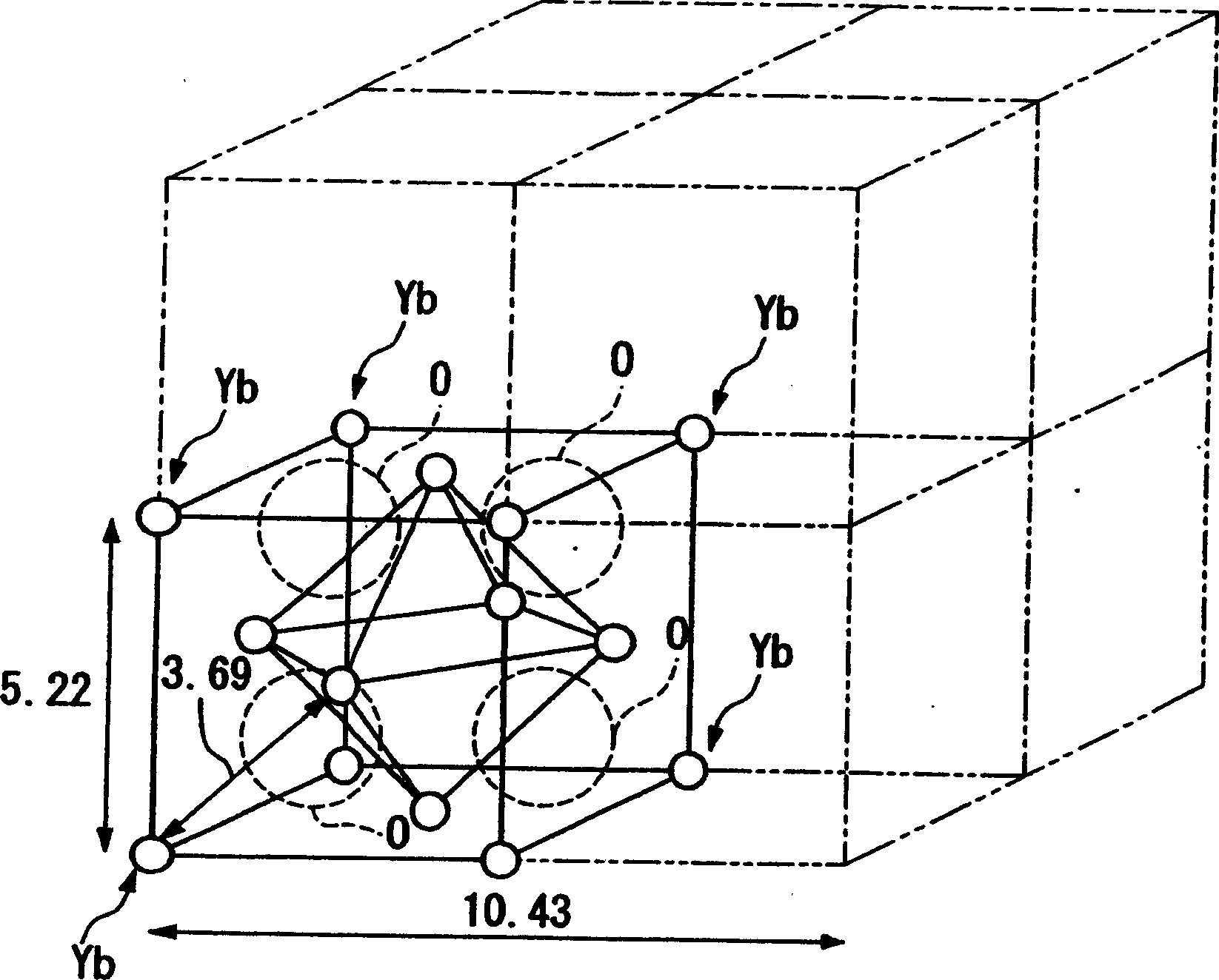
[0091] use Figure 4 The device for producing polycrystalline thin films is shown, in which the pressure in the film forming chamber is reduced to 3.0×10 by exhausting using a rotary pump and a cryopump. -4 Torr (4×10 -2 Pa), a mirror-polished nickel-based alloy C276 tape with a width of 10 mm, a thickness of 0.5 mm, and a length of 100 cm was used as a tape-shaped substrate. Use containing Yb 2 o 3 target, the sputtering voltage was set at 1000V, the sputtering current was set at 100mA, and the Kr ejected from the ion source + The incident angle of the ion beam to the normal of the film forming surface was set at 55 degrees, the transmission distance of the ion beam was set at 40 cm, the sputtering voltage of the ion beam was set at 150 eV, and the current density of the ion beam was set at 100 μA / cm 2 , moreover, when the temperature of the substrate strip was set to 300 °C and the oxygen inflow to 1×10 -4 Torr (1.3×10 -2 In the environment of Pa), the constituent part...


PUM

PropertyMeasurementUnit
current densityaaaaaaaaaa
thicknessaaaaaaaaaa

Abstract

In the production method for a polycrystal thin film, when a polycrystal thin film is deposited on a polycrystal base material, the temperature of the polycrystal base material is set to the range of 150 to 250[deg.]C, the ion beam energy of an ion beam is controlled to the range of 175 to 225eV, and the ion beam is applied to the normal of the face to be film-formed in the polycrystal base material at an incident angle of 50 to 60 degrees. By the production method, the polycrystal thin film in which the inclination of grain boundaries composed by the same crystal axes of the crystal grains of the polycrystal thin film along the face parallel to the face to be film-formed in the polycrystal base material is suppressed to <=20 degrees, and having high crystal orientation properties can stably be produced.

Description

technical field [0001] The present invention relates to a method for producing a polycrystalline thin film containing the crystalline structure of C-type rare earth oxides in a well-arranged crystal arrangement. The present invention also relates to a method for producing an oxide superconductor containing the above-provided Polycrystalline film and oxide superconducting layer have excellent superconducting properties. Background technique [0002] Oxide superconductors discovered in recent years are excellent superconductors whose critical temperature exceeds the temperature of liquid nitrogen, but at present, in order for such oxide superconductors to be practically used, various problems described below must be solved. One of the problems is that the critical current density of oxide superconductors is very low. The main reason for the low current density is the inherent anisotropic electrical properties of oxide superconductors. In particular, it has been well known th...

Claims


Application Information

Patent Timeline
Patent Type & Authority Applications(China)
IPC IPC(8): C23C14/08C23C14/34C23C14/46H01L39/24
CPCC23C14/087H01L39/2461C23C14/46C23C14/3442C23C14/08H01L39/2448H10N60/0521H10N60/0632
Inventor 饭岛康裕
Owner THE FUJIKURA CABLE WORKS LTD
Learn More