


Quick Research
Generate reliable direction feasibility study reports for your R&D in just a few steps.

Technical Q&A
Discover and master advanced knowledge NOW. Basics, ideas, possibilities, all at once.

Find Solutions
As an expert in R&D theories, this can generate solutions to your technical problems instantly.

Evaluate Feasibility
Analyze your overall solution with one click, know your potential R&D risks in advance.

Monitor Landscape
Get weekly tech updates, stay abreast of the latest tech innovations and key insights.
Method and device for stripping semiconductor device by ring-type contact unit
A technology of a ring-shaped contact and peeling device, which is applied in the fields of semiconductor devices, semiconductor/solid-state device manufacturing, electric solid-state devices, etc., can solve the problems of easily damaged silicon chips 16 and difficult to peel off silicon chips 16, etc.
- Summary
- Abstract
- Description
- Claims
- Application Information
AI Technical Summary
Problems solved by technology
Method used
Image

Examples
Embodiment Construction
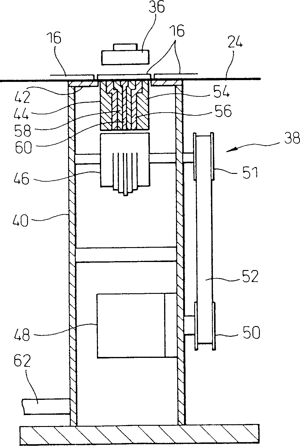
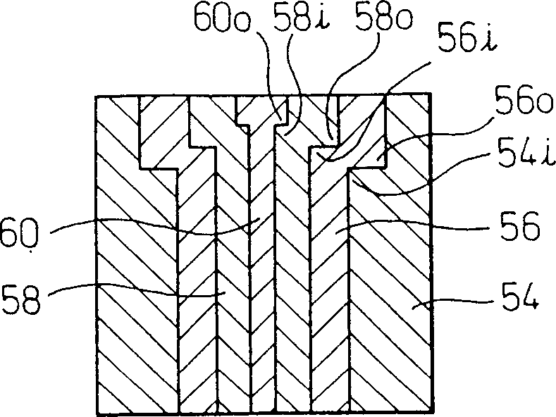
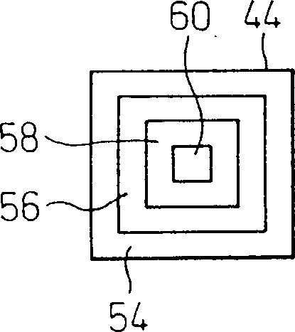
[0033] Embodiments of the present invention will be described below with reference to the drawings. specific reference Figure 10A-1 0F, a typical example illustrating a series of steps of a method of manufacturing a semiconductor device.
[0034] Figure 10A is a view showing a silicon wafer (semiconductor substrate) undergoing an integrated circuit manufacturing process. The silicon wafer 10 has a first surface 12 and a second surface 14 on which a number of semiconductor elements (silicon chips) 16 have been formed during the integrated circuit manufacturing process. exist Figure 10B In the process, the protective tape 18 is bonded on the first surface 12 of the silicon wafer 10 .
[0035] exist Figure 10C In the process, the second surface 14 of the silicon wafer 10 is ground while the protective tape 18 is adhered to the first surface 12 of the silicon wafer 10 . In this example, a diamond grinding wheel 22 serving as a machining tool grinds the second surface of ...
PUM
 Abstract
Description
Claims
Application Information
 - R&D Engineer
- R&D Manager
- IP Professional
- Industry Leading Data Capabilities
- Powerful AI technology
- Patent DNA Extraction
Browse by: Latest US Patents, China's latest patents, Technical Efficacy Thesaurus, Application Domain, Technology Topic, Popular Technical Reports.
© 2024 PatSnap. All rights reserved.Legal|Privacy policy|Modern Slavery Act Transparency Statement|Sitemap|About US| Contact US: help@patsnap.com