Film capacitor
A technology of film capacitors and capacitors, applied in the direction of film/thick film capacitors, laminated capacitors, fixed capacitor dielectrics, etc., can solve problems such as difficult to apply frequency areas
- Summary
- Abstract
- Description
- Claims
- Application Information
AI Technical Summary
Problems solved by technology
Method used
Image
Examples
Embodiment 1
[0024] In Example 1, a case where a metal foil is used as an electrode layer will be described. In the capacitor element at this time, polyethylene terephthalate, polyphenylene sulfide, or polyphenylene naphthalate is used as a dielectric film, and as an electrode layer As the material, metal foil such as aluminum foil or an alloy containing aluminum is used.
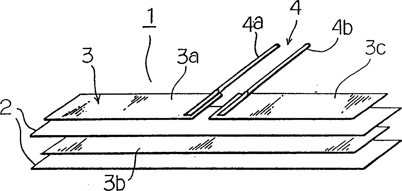
[0025] Common lead wires such as copper plating (CP: copper plating) wires are used for the lead-out connectors. A wound type series capacitor element 1 using the above material is placed in figure 1 In the figure, the coiled state is unwrapped and stretched.
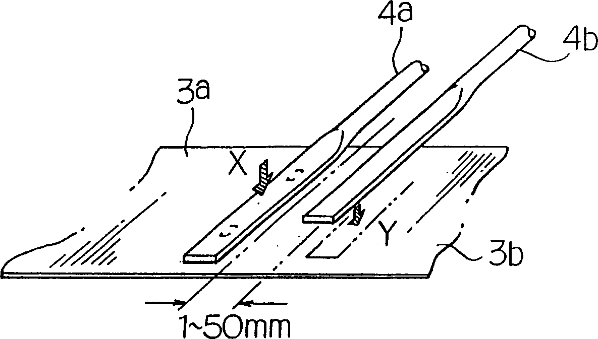
[0026] figure 1 In the capacitor element 1, the insulating layer 2 composed of two strip-shaped dielectric films and the electrode layer 3 composed of a pair of aluminum foils alternated up and down are superimposed. Either one of the upper and lower electrodes (here, the upper side) of the electrode layer 3 is divided into two parts, and arranged in the lo...
Embodiment 2
[0032] In Example 1 above, the case where metal foil such as aluminum or the like was used for all electrode layers 3 was described. In Example 2, the structure in which the electrode layer is a combination of metal foil and a metallized film made of vapor-deposited metal is described. .
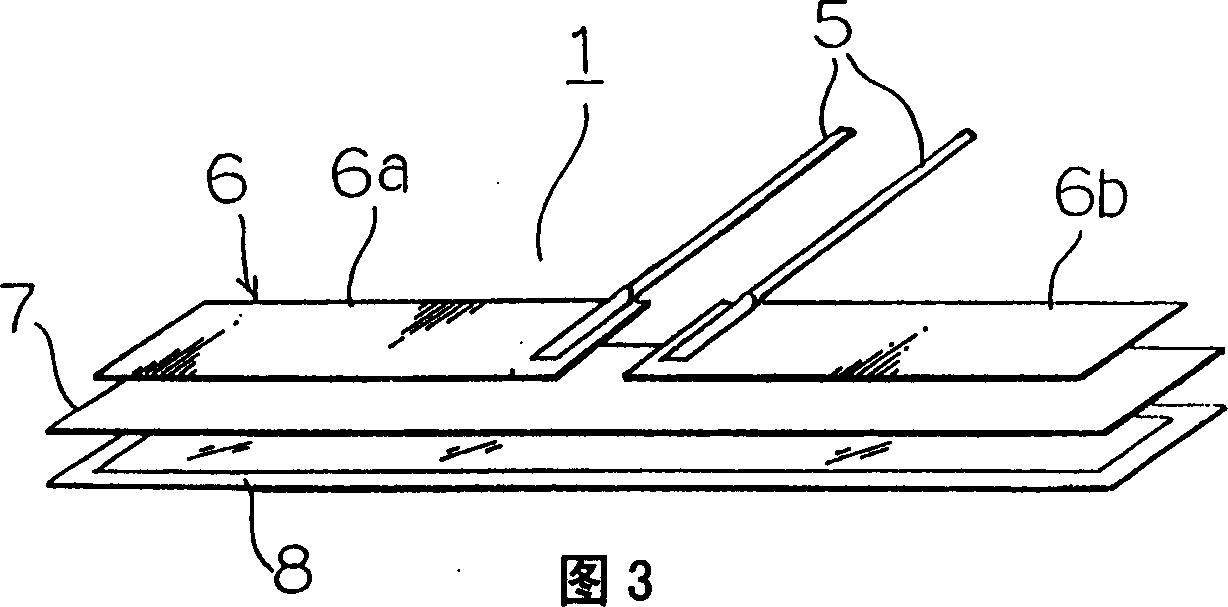
[0033] At this time, as shown in FIG. 3 , the electrode layer 6 on the lead wire 5 side is made of metal foil, and the electrode layer 8 on the opposite side with the dielectric film 7 is made of a metallized film. In addition, the attachment position of the lead wire 5 is set to the side where the electrode layer 6a and the electrode layer 6b are adjacent to each. In addition, the adjacent interval between the electrode layers 6a and 6b is set to 1 to 50 mm.
[0034] In addition, in the element structure at this time, the positional relationship between the metal foil, the dielectric film, and the metallized film, in addition to the above-mentioned FIG. Figure 4 The metal foil 6, the met...
Embodiment 3
[0037] FIG. 5 shows a capacitor element 1 according to Example 3 of the present invention. As shown in FIG. 5 , one electrode layer 9 is divided in the width direction (slits are provided in the winding direction). That is, the electrode layers 9 a and 9 b are formed by dividing in a direction of 90° with respect to the lead-out direction. Further, one of them is divided in the longitudinal direction, and lead wires 10 are formed on the divided electrode layers 9a and 9c, respectively. Even in this case, the lead wires 10 are attached at positions adjacent to the electrode layers 9a and 9c, respectively. In addition, another electrode layer 9d is divided in the longitudinal direction. Here, it is divided into 2 parts.
[0038] In addition, FIG. 5 shows a state in which the capacitor element 11 is not wound, and the dotted line in the figure shows a simulation of a current path.
[0039] The capacitor element 11 composed of such an element structure is stacked and wound wit...
PUM
 Abstract
Description
Claims
Application Information
 - R&D Engineer
- R&D Manager
- IP Professional
- Industry Leading Data Capabilities
- Powerful AI technology
- Patent DNA Extraction
Browse by: Latest US Patents, China's latest patents, Technical Efficacy Thesaurus, Application Domain, Technology Topic, Popular Technical Reports.
© 2024 PatSnap. All rights reserved.Legal|Privacy policy|Modern Slavery Act Transparency Statement|Sitemap|About US| Contact US: help@patsnap.com


