
Method for producing printing cream for electrode jump absorption, laminating ceramics electronic component

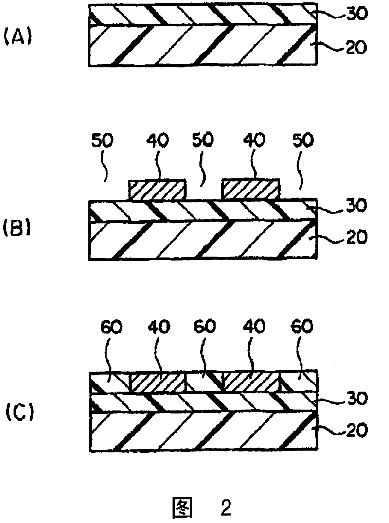
A technology of electronic components and printing paste, which is applied in the field of printing paste for electrode step absorption, which can solve the problems of sheet erosion and achieve the effects of preventing sheet erosion, improving peelability, and reducing short-circuit faults

Inactive Publication Date: 2011-11-16
TDK CORPARATION
View PDF1 Cites 0 Cited by
  • Summary
  • Abstract
  • Description
  • Claims
  • Application Information

AI Technical Summary

Problems solved by technology

[0014] However, although various solvents with such a high effect of preventing sheet erosion can prevent sheet erosion at room temperature, when the temperature rises to the drying temperature of the solvent (for example, 40 to 90°C), sheet erosion will occur. Erosion, therefore, tends to also erode green sheets when solvent-dried

Method used


Image

  • Method for producing printing cream for electrode jump absorption, laminating ceramics electronic component
  • Method for producing printing cream for electrode jump absorption, laminating ceramics electronic component
  • Method for producing printing cream for electrode jump absorption, laminating ceramics electronic component

Examples


Embodiment approach

[0109] As mentioned above, although embodiment of this invention was described, this invention is not limited to the said embodiment, Various changes are possible in the range which does not deviate from the summary of this invention.

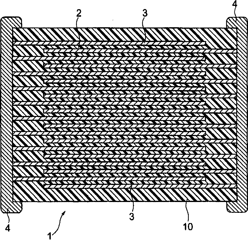
[0110] For example, the above embodiments exemplify multilayer ceramic capacitors as the multilayer ceramic electronic components of the present invention, but the multilayer ceramic electronic components of the present invention are not limited to multilayer ceramic capacitors, and can of course be applied to multilayer ceramic substrates and the like.

Embodiment 1

[0114] First, a butyral resin-containing dielectric paste for forming a ceramic green sheet using a butyral resin (polyvinyl butyral) as an organic binder was prepared.

[0115] Preparation of Dielectric Paste Containing Butyral Resin

[0116] Prepare BaTiO 3 Ceramic powder, polyvinyl butyral (PVB) as an organic binder, and methanol as a solvent. Then, 10 parts by weight of the organic binder and 150 parts by weight of the solvent were weighed with respect to 100 parts by weight of the ceramic powder, and kneaded and slurried by a ball mill to obtain a butyral resin-containing dielectric paste.

[0117] Fabrication of Ceramic Green Sheets Containing Butyral Resin

[0118] The above-mentioned dielectric paste was applied to a predetermined thickness on a PET film by a doctor blade method, and dried to form a butyral resin-containing ceramic green sheet having a thickness of 1.5 μm after drying.

[0119] Compatibility test of solvent and ceramic chip containing butyral ...

Embodiment 2

[0127] Compatibility test of solvent and ceramic green sheet containing acrylic resin (50°C, dipping)

[0128] Except using acrylic resin as the organic binder, operate in the same manner as in Example 1 to make a dielectric paste containing acrylic resin and a ceramic green sheet containing acrylic resin. Compatibility test of green sheet (50°C, immersion).

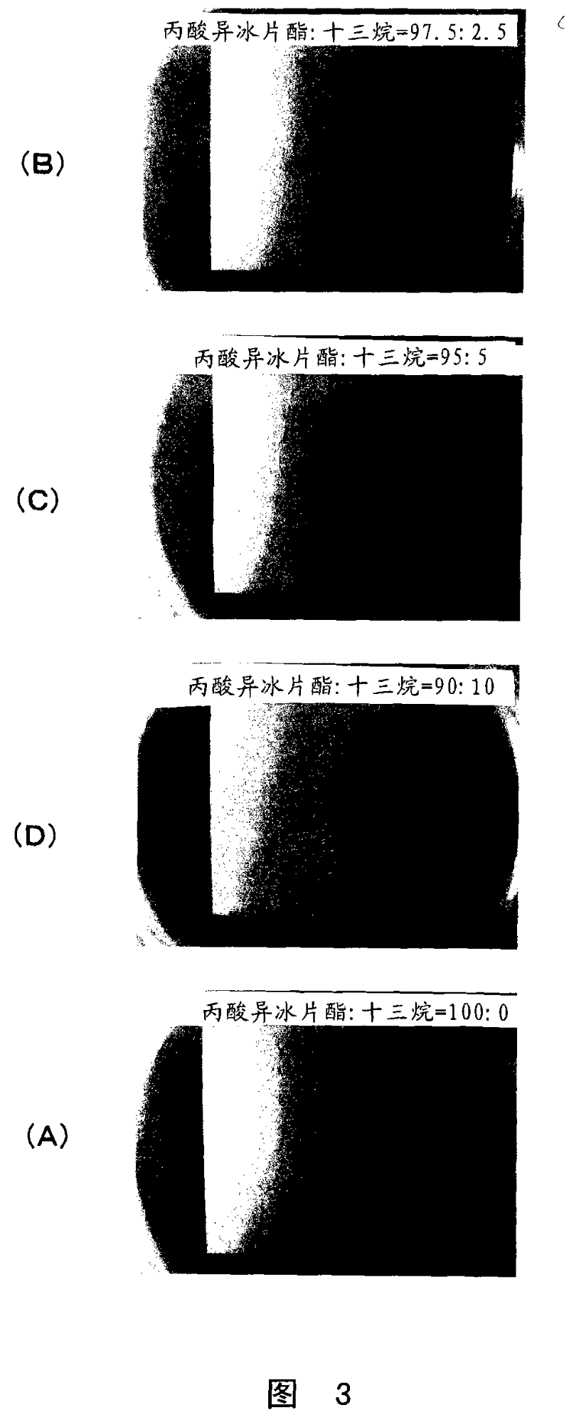
[0129] In addition, in Example 2, various solvents shown in Table 2 below were used as solvents, and photographs of acrylic resin-containing ceramic green sheets dipped in the respective solvents were shown in each figure described in Table 2, respectively.

[0130] Table 2

[0131] solvent microscope photo Isobornyl propionate: tridecane = 100:0 Figure 5 (A) Isobornyl propionate: tridecane = 97.5: 2.5 Figure 5 (B) Isobornyl propionate: tridecane = 95:5 Figure 5 (C) Isobornyl propionate: tridecane = 90:10 Figure 5 (D)

[0132] Depend on Figure 5 (B)~ ...


PUM

PropertyMeasurementUnit
thicknessaaaaaaaaaa
thicknessaaaaaaaaaa
particle sizeaaaaaaaaaa

Abstract

The invention provides a printing paste used in the absorption of an electrode scale and for manufacturing a laminated ceramic electronic component. The invention is characterized in that the printing paste is used together with a ceramic plate which contains the butyral resin or the acrylic resin and has a thickness of less than 5Mum and contains ceramic powder and organic paint vehicle, wherein, the solvent of the organic paint vehicle contains a aliphatic hydrocarbon which is selected form one or more of the isobornyl acrylate, the isoamyl butyrate and the isobornyl isobutyrate and a carbon atomicity ranging from 5 to 40. The invention provides the printing paste used in the absorption of an electrode scale and for manufacturing a laminated ceramic electronic component. When the ceramic plate becomes thinner, even in the temperature (for example 40-90 DEG C) for the drying of the solvent, the sheet can be effectively prevented from being eroded, so the case in the room temperature does not need to be mentioned.

Description

technical field [0001] The present invention relates to a printing paste (pate) for absorbing electrode steps used for manufacturing laminated ceramic electronic components and a method for manufacturing laminated ceramic electronic components using the paste. Background technique [0002] A multilayer ceramic capacitor, which is an example of a multilayer ceramic electronic component, is usually produced by forming a ceramic green sheet on a carrier sheet using a dielectric paste by the squeegee method or the like, and printing a green sheet for internal electrode formation on it in a predetermined pattern. Conductive paste, let it dry to form the internal electrode pattern. Then, the ceramic green sheet is peeled off from the carrier sheet, and laminated to a desired number of layers. [0003] At this time, two lamination methods involving a method of peeling the ceramic green sheet from the carrier sheet before lamination and a method of peeling the carrier sheet after l...

Claims


Application Information

Patent Timeline
Patent Type & Authority Patents(China)
IPC IPC(8): H01G4/002H01G4/30H01F17/00
CPCC04B35/62218C04B35/6342C04B35/6365H01G4/1209H01G4/30
Inventor 三浦秀一小田和彦丸野哲司
Owner TDK CORPARATION
Learn More