Tester with magnetic tunnel junction and magnetioelectric resistance material for 3D weak magnetic field
A magnetic tunnel junction and weak magnetic field technology, which is applied in the field of three-dimensional weak magnetic field detection devices, can solve the problems of fast response time and achieve high sensitivity, magnetic moment reset and demagnetization, and high detection effects
- Summary
- Abstract
- Description
- Claims
- Application Information
AI Technical Summary
Problems solved by technology
Method used
Image
Examples
example 1
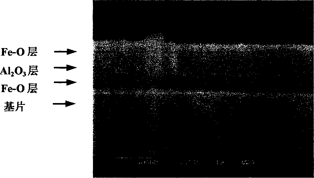
[0036] Example 1: A magnetic tunnel junction magnetoresistive chip sensitive to a single direction magnetic field, composed of a three-layer film of the magnetic tunnel junction magnetoresistance sensing part and a double-layer film of a conductive thin film, is fabricated on a quartz glass substrate.
[0037] After the above-mentioned substrate with a length of 10 mm, a width of 10 mm and a thickness of 0.5 mm is ultrasonically cleaned with acetone, ultrasonically cleaned with deionized water, and finally ultrasonically cleaned with absolute ethanol. After cleaning, the substrate was blown dry with high-purity nitrogen gas. Put the cleaned substrate into the coating chamber of the magnetron sputtering coating equipment, pump the coating chamber to 2×10 -4 Pascal's vacuum. Deposit a 500 nm thick copper film on the substrate by magnetron sputtering, the working gas is 0.8 Pascal argon, and subsequently deposit a 200 nm thick silicon dioxide film on it by radio frequency magnet...
example 2
[0040] Example 2: A magnetic tunnel junction magnetoresistive chip sensitive to a single direction magnetic field, composed of a magnetic tunnel junction magnetoresistance four-layer film and a conductive thin film strip double layer film, was fabricated on a thermally oxidized silicon substrate.
[0041] The above-mentioned thermally oxidized silicon substrate with a length of 10 mm, a width of 10 mm, and a thickness of 0.5 mm (the thickness of the silicon dioxide layer on the silicon surface is 500 nanometers) is ultrasonically cleaned with acetone, then ultrasonically cleaned with deionized water, and finally ultrasonically cleaned with absolute ethanol. After cleaning, the substrate was blown dry with high-purity nitrogen gas. Put the cleaned substrate into the coating chamber of the magnetron sputtering coating equipment, pump the coating chamber to 2×10 -4 Pascal's vacuum. Deposit a 500 nanometer thick copper film on the substrate by magnetron sputtering, the working ga...
PUM
| Property | Measurement | Unit |
|---|---|---|
| thickness | aaaaa | aaaaa |
| thickness | aaaaa | aaaaa |
| size | aaaaa | aaaaa |
Abstract
Description
Claims
Application Information
 - R&D
- Intellectual Property
- Life Sciences
- Materials
- Tech Scout
- Unparalleled Data Quality
- Higher Quality Content
- 60% Fewer Hallucinations
Browse by: Latest US Patents, China's latest patents, Technical Efficacy Thesaurus, Application Domain, Technology Topic, Popular Technical Reports.
© 2025 PatSnap. All rights reserved.Legal|Privacy policy|Modern Slavery Act Transparency Statement|Sitemap|About US| Contact US: help@patsnap.com


